Spikiera
Newbie level 2

- Joined
- Jul 28, 2011
- Messages
- 2
- Helped
- 0
- Reputation
- 0
- Reaction score
- 0
- Trophy points
- 1,281
- Activity points
- 1,305
Hello everyone,
I am having some serious issue trying to use a single JK flip flop to build a frequency divider (divide by 2). Somehow my output "Q" either does not toggle at all or toggles at the wrong frequency. Or, the output just doesn't make sense.
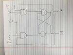
The JK flip flop I use looks like the following:

It is a 4 NAND gates JK FF. I tie both J and K node to VDD, and the CLK is my input. According to many textbook or on-line resources, the output should toggle at half of the CLK frequency.
I run the design in Cadence analog design environment but the output just doesn't toggle correctly. The NAND gates are CMOS NAND gate...3 parallel PMOS pull up and 3 series NMOS pull down for example. All 4 NAND gates use the same sizing.
It is driving me crazy, I've worked on this the whole day. I am now doubting this topology even works. It looks like it is difficult to maintain good oscillation and the feedback usually can destroy the way the signal toggles. It doesn't look like an edge trigger FF either. I think DFF would work much better, but has anyone done this before and worked?
I cannot figure out the timing requirements for each gate, is the timing for the 4 NAND gate very very important?
Please help....:bang::bang::bang:
Thank you guys so much!
I am having some serious issue trying to use a single JK flip flop to build a frequency divider (divide by 2). Somehow my output "Q" either does not toggle at all or toggles at the wrong frequency. Or, the output just doesn't make sense.
The JK flip flop I use looks like the following:

It is a 4 NAND gates JK FF. I tie both J and K node to VDD, and the CLK is my input. According to many textbook or on-line resources, the output should toggle at half of the CLK frequency.
I run the design in Cadence analog design environment but the output just doesn't toggle correctly. The NAND gates are CMOS NAND gate...3 parallel PMOS pull up and 3 series NMOS pull down for example. All 4 NAND gates use the same sizing.
It is driving me crazy, I've worked on this the whole day. I am now doubting this topology even works. It looks like it is difficult to maintain good oscillation and the feedback usually can destroy the way the signal toggles. It doesn't look like an edge trigger FF either. I think DFF would work much better, but has anyone done this before and worked?
I cannot figure out the timing requirements for each gate, is the timing for the 4 NAND gate very very important?
Please help....:bang::bang::bang:
Thank you guys so much!

