Continue to Site

Welcome to EDAboard.com

Welcome to our site! EDAboard.com is an international Electronics Discussion Forum focused on EDA software, circuits, schematics, books, theory, papers, asic, pld, 8051, DSP, Network, RF, Analog Design, PCB, Service Manuals... and a whole lot more! To participate you need to register. Registration is free. Click here to register now.

[PIC] Issue in driving MOSFET for Dual supply

Status
Not open for further replies.

NIDHINDAS

Newbie level 6
Newbie level 6
Joined
Sep 30, 2010
Messages
12
Helped
0
Reputation
0
Reaction score
1
Trophy points
1,283
Activity points
1,398
Hello,

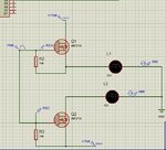
PFA for the design using FAN-7392 to drive dual supply power with the dual load(battery) connected in series (+.........-+..........- ).
The microcontroller is PIC16F877A with separate Two PWM driving positive side and negative side MOSFET independently.
MCUs ground is -17 volt, not 0 of dual supply, to measure -ve volt as positive.
The issue is Q1 is not conducting now, what may be the reasons?
Q2 is working now.

2. MCUs can't measure -ve voltages how this is taken care of in the situation it needs.

Thanks in advance.

Regards,
Nidhindas
 

Attachments

  • Capture.JPG
    Capture.JPG
    96.7 KB · Views: 167

Hi,

Low side transistor is ON all the time.
The IC is not suitable to control negative load voltages.

What's your expected switching frequency?
What's your expected duty cycle range?

Klaus
 

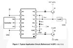
The problem is your arbitrary modification of the original application circuit

1605512751430.png


1. COM has to be connected to Q2 emitter.
2.The IC allows only a limited voltage shift between Vss and COM.

The datasheet specifies a "VSS Logic supply offset voltage", minimal VCC - 25, maximal VCC + 0.3.
 

Hi,

Yes, I did not recognize the allowed voltage offset before.
But it's limited to abs. Max of 25V wrt low side supply.
Low side supply now is 15V, thus the lowest voltage is -10V.

--> with -17V is still can't work.

The recommended offset is +/-5V only, I guess just to compensate for ground bouncing in high power applications.

Klaus
 

Hi,

Low side transistor is ON all the time.
The IC is not suitable to control negative load voltages.

What's your expected switching frequency?
What's your expected duty cycle range?

Klaus

What's your expected switching frequency?
Around 20khz to 50khz
What's your expected duty cycle range?
0% to 80% max
 

But it's limited to abs. Max of 25V wrt low side supply.
Low side supply now is 15V, thus the lowest voltage is -10V.

--> with -17V is still can't work.

The recommended offset is +/-5V only, I guess just to compensate for ground bouncing in high power applications.
I think, the design flow is different:

1. Low side supply needs common ground with Q2 emitter. This is required for correct Q2 gate voltage and operation of the bootstrap supply.
2. Supply voltage level is decided according to IGBT gate drive requirements.
3. Depending on the offset between Vcc and controller ground, you possibly need a level shifter for the input signal and a respective separate Vdd supply.
 

Hi,

1) agreed
2) agreed
3) agreed

:)
 

The problem is your arbitrary modification of the original application circuit

View attachment 165709

1. COM has to be connected to Q2 emitter.
2.The IC allows only a limited voltage shift between Vss and COM.

The datasheet specifies a "VSS Logic supply offset voltage", minimal VCC - 25, maximal VCC + 0.3.

1. COM has to be connected to Q2 emitter.
If COM is -17volt (consider VSS=+17 and COM is -17 volt)or we can consider this as equivalent to single-ended supply 34 --0 volts?.
2.The IC allows only a limited voltage shift between Vss and COM.
Yes , VSS= 34 and COM =0 but as (+17 to -17).

The datasheet specifies a "VSS Logic supply offset voltage", minimal VCC - 25, maximal VCC + 0.3.
There are 3 voltages here
VDD ---VSS (5-0 volts) logic voltage from MCU
VCC --- COM(15-0volts) supply for MOSFET driver
(+17)----(-17) Driven voltage

And in all above 0 is using as -17 volt only
--- Updated ---

I think, the design flow is different:

1. Low side supply needs common ground with Q2 emitter. This is required for the correct Q2 gate voltage and operation of the bootstrap supply.
2. Supply voltage level is decided according to IGBT gate drive requirements.
3. Depending on the offset between Vcc and controller ground, you possibly need a level shifter for the input signal and a respective separate Vdd supply.

1. Low side supply needs common ground with Q2 emitter. This is required for the correct Q2 gate voltage and operation of the bootstrap supply.
Yes, common ground is there here its -17 volt (-volt we cannot consider here as we do not reference this volt to real GND ).
2. Supply voltage level is decided according to IGBT gate drive requirements.
yes, the VGS threshold is a minimum of 8 volts for proper conduction.
3. Depending on the offset between Vcc and controller ground, you possibly need a level shifter for the input signal and a respective separate Vdd supply.
This issue is not there now.

For reference, I have attached a simplified "Design1.jpg " image, this only I am trying to achieve.
I will post a detailed circuit in the upcoming days. Please help.
 

Attachments

  • Capture.JPG
    Capture.JPG
    97 KB · Views: 124
  • Design1.JPG
    Design1.JPG
    91 KB · Views: 137
Last edited:

Please check the supply voltages. Maxiumum ratings of driver and IGBT are exceeded.
 

The issue is Q1 is not conducting now, what may be the reasons?

Pin 7 must provide from +8 to +17 V in order to fully turn on Q1. Perhaps with bootstrapping it does so?

When Q1 conducts, pin 5 receives 17 V. Is this normal operation?
Does Q1 conducting cause pin 6 voltage to change? Is this normal operation?
 

Status
Not open for further replies.

Similar threads

Part and Inventory Search

Welcome to EDABoard.com

Sponsor

Back
Top