Continue to Site

Welcome to EDAboard.com

Welcome to our site! EDAboard.com is an international Electronics Discussion Forum focused on EDA software, circuits, schematics, books, theory, papers, asic, pld, 8051, DSP, Network, RF, Analog Design, PCB, Service Manuals... and a whole lot more! To participate you need to register. Registration is free. Click here to register now.

Is this a correct implementation of a JK flip flop

tiredstudent

Newbie
Newbie level 1
Joined
Mar 13, 2024
Messages
1
Helped
0
Reputation
0
Reaction score
0
Trophy points
1
Activity points
14
I'm getting started in digital electronics and I've never seen an implementation of a flip flop JK like the one I did. I know its not optimal, but is it ok? the NAND version and the one using a latch SR are not easy to came up with for me. I feel like I need to just remember them, while this implemetation is easy to get when you know how the FF works
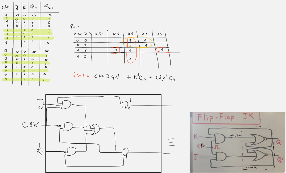
Screenshot 2024-03-13 at 00-46-13 Electronica.png
 
I don't understand the left schematic. Q' is not even driven, how can it be equivalent to right schematic?

In my systematic, a level sensitive storage element is a latch rather than a flip-flop.
 

LaTeX Commands Quick-Menu:

Part and Inventory Search

Welcome to EDABoard.com

Sponsor

Back
Top