d123
Advanced Member level 5

Hi,
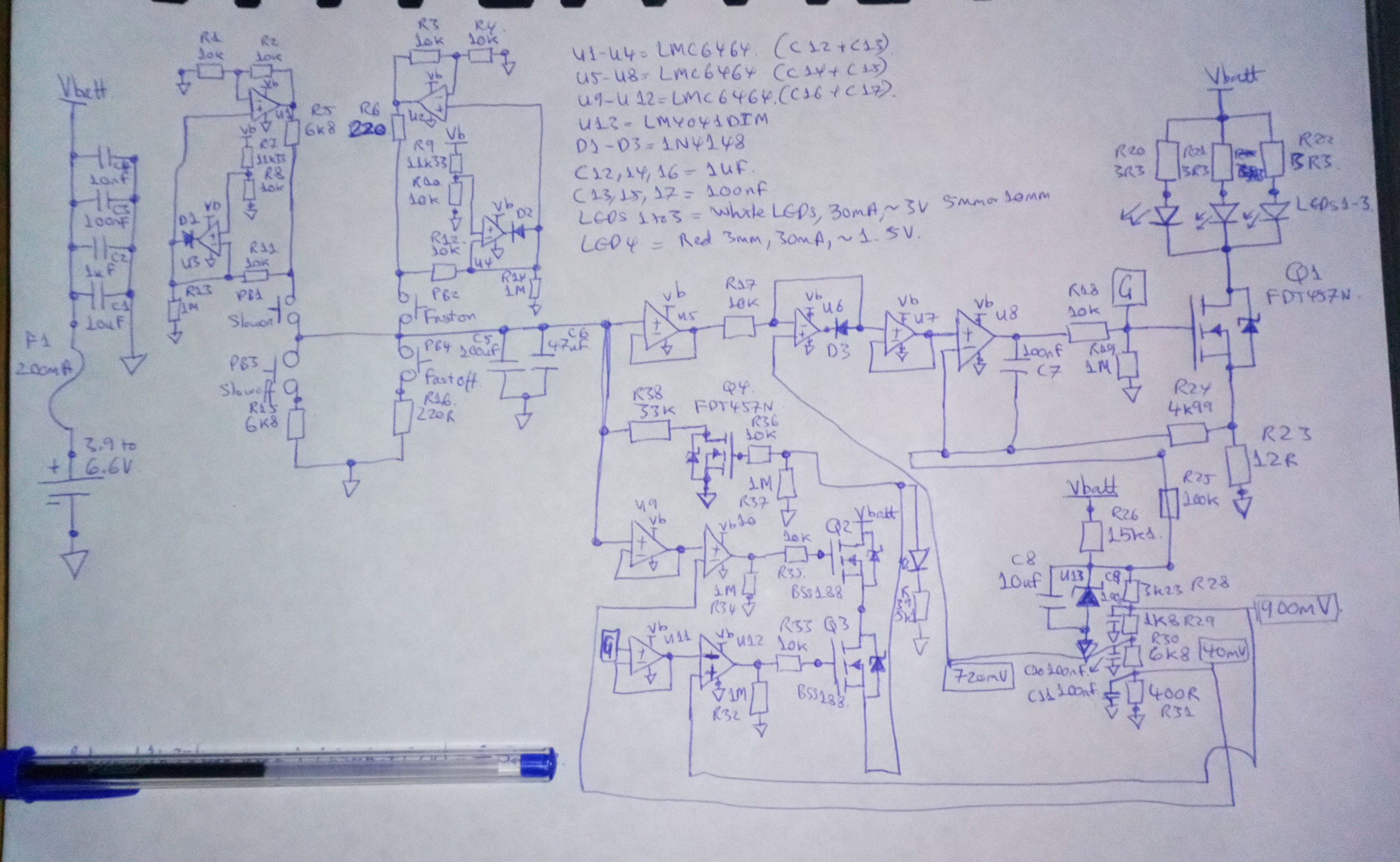
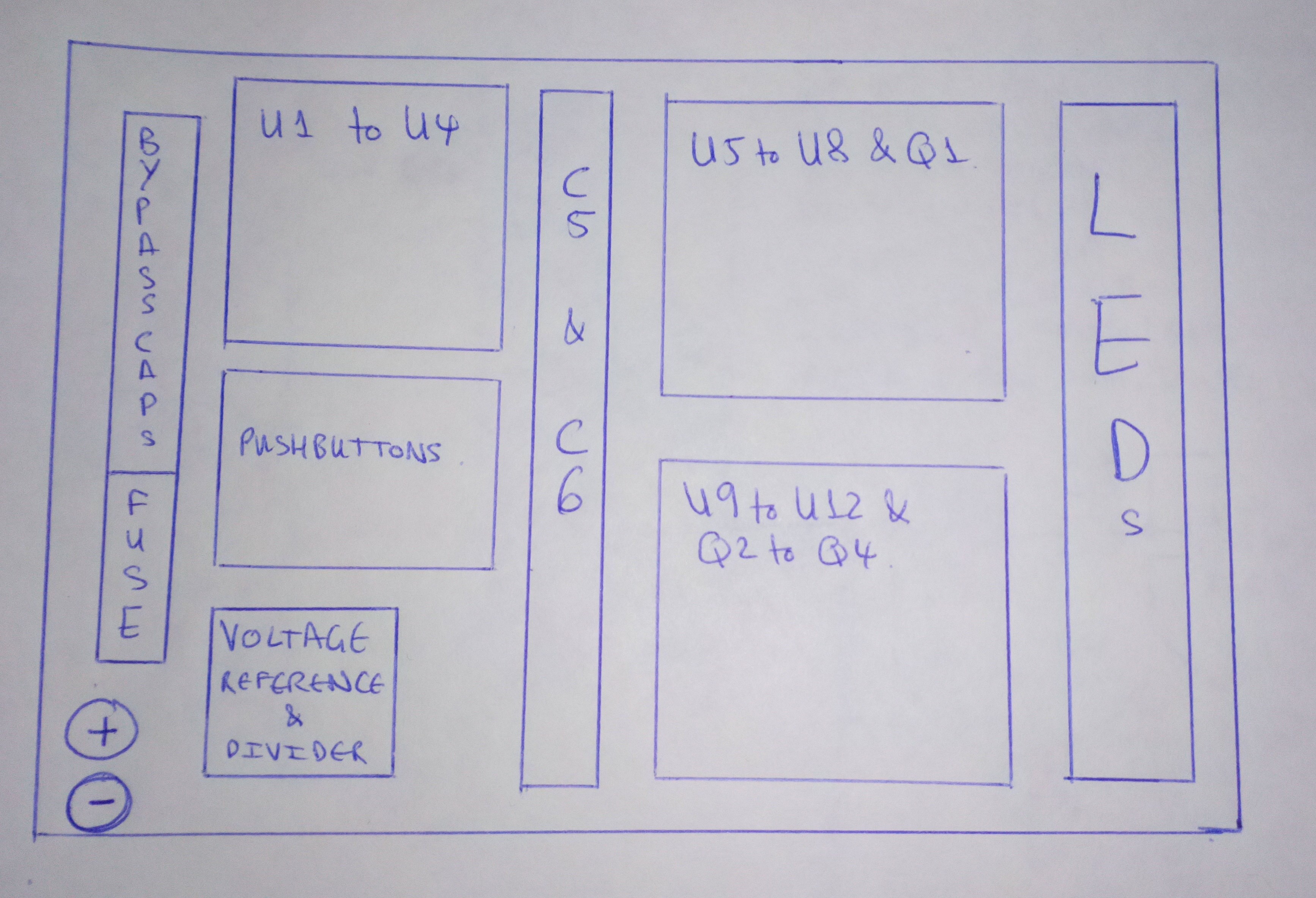
Is this pcb layout plan right for a single-sided 35 um copper-clad fr4 board which will have an uninterrupted ground plane and most signals routed on same side (some positive power connections will be made with jumper wires if they would otherwise cut off the ground plane)?
Vref close to supply + and - connections, noisiest part of circuit (return current of ~60mA) at other side of board. C5 and C6 are a long strip as will either use multiple 10uF 1206 X7R capacitors or much less space with three 47uF - I think, size-wise - 5012 tantalum capacitors.
Is that right or should noisiest section be as close to battery negative connection point and Vref at other end of pcb, or doesn't it matter either way with a solid/uninterrupted ground plane?
Thanks.

