Continue to Site

Welcome to EDAboard.com

Welcome to our site! EDAboard.com is an international Electronics Discussion Forum focused on EDA software, circuits, schematics, books, theory, papers, asic, pld, 8051, DSP, Network, RF, Analog Design, PCB, Service Manuals... and a whole lot more! To participate you need to register. Registration is free. Click here to register now.

Inverter design problem

Status
Not open for further replies.

clicco89

Newbie level 4
Newbie level 4
Joined
Apr 30, 2018
Messages
7
Helped
0
Reputation
0
Reaction score
0
Trophy points
1
Activity points
61
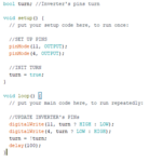
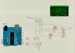
Hi, I'm trying to design an Inverter based on arduino, here's the schematic and the code:
Cattura1.PNG
Cattura2.PNG
The problem is that, measuring the voltage right after Q1 and Q2, I get a strange graph as you can see in the first image, here's the graph I expected:
Cattura3.png
My question is why do I get that?
Sorry if I asked a stupid question, but I'm still learning electronics.
Thank you in advance for the answers.
 

Hi,

without knowing any voltage of your applicaiton ... all we can do is guess.

****
Why making life harder than necessary?
High side siwtiching usually is more complicated than low side switching.
You will find a lot of similar applications all with low side switch....where the center tap of the tranformer is connected with the positive supply rail.

Klaus
 

You swapped the PMOS source and drain. Protection diode is forward biased.
 

Hi,

true.

and even then there are some issues:
* cross conducting: There is a short time every cycle where both MOSFETs are ON. Causing short circuit currents to flow.
* this needs 100% of processing time. The microcontroller is not able to do anything else without causing probems with the tranformer.

Klaus
 

The fundamental problem is the Arduino output is probably below the Vgs threshold of the MOSFETS anyway and certainly won't be enough to drive them to full conduction, especially with the load in the source pin. Remember that the gate has to be above the source voltage by >Vgs threshold before it even starts to conduct, consider how that would be possible if you already raised the primary voltage to push current into the transformer.

You might be able to connect +V to the transformer center, with the drain pins to the ends and source to ground but I would still have serious reservations about drive levels unless you employ an additional driver stage. As Klaus points out, you also need a 'dead time' at the start of the next MOSFET turning on so there is no chance of both being conductive at the same time.

Brian.
 

Hi,

The circuit needs a level shifter which would be a gate driver IC suited to 3.3V logic level inputs, if not a level shifter (a BJT or a logic level MOSFET with a very low VGSth ON) followed by a gate driver IC. I would even consider placing a cheap optocoupler between that MOSFET and the nasty transformer and the pretty little delicate Arduino - I doubt the Arduino will enjoy that circuit, to be honest...
 

Hi, thank you all for the answers!
I changed my circuit and code like this:
Cattura1.PNG
Cattura2.PNG
Now it works, I added a level shifter and made inverter's controller asynchronous to use the arduino for other purposes also.
Do you have any suggestion left?
 

Status
Not open for further replies.

Part and Inventory Search

Welcome to EDABoard.com

Sponsor

Back
Top