Continue to Site

Welcome to EDAboard.com

Welcome to our site! EDAboard.com is an international Electronics Discussion Forum focused on EDA software, circuits, schematics, books, theory, papers, asic, pld, 8051, DSP, Network, RF, Analog Design, PCB, Service Manuals... and a whole lot more! To participate you need to register. Registration is free. Click here to register now.

[SOLVED] Interfacing STM32F429 (FMC) with a 1 GB Parallel NOR Flash (M29EWL)

Status
Not open for further replies.

e-music

Member level 5
Member level 5
Joined
Dec 29, 2017
Messages
84
Helped
0
Reputation
0
Reaction score
0
Trophy points
6
Activity points
1,065
Interfacing STM32F429 (FMC) with a 1 GBit Parallel NOR Flash (M29EWL)

Hello Folks!

I'm trying to interface a 1 GBit parallel NOR flash with an STM32F429 microcontroller through the FMC peripheral. The full part number is: JS28F00AM29EWLA. Here is the datasheet: View attachment m29ew_256mb_2gb.pdf

The problem is, the 256 MB (2 Gbit) address space dedicated to the first bank of the FMC peripheral for the NOR/SRAM memories is divided across 4 sub banks, 64 MB each with an individual NEx (chip select) signal for each sub-bank.

As I can see, STM32CubeMX has no problem configuring a single sub-bank with 26 address bits. However, accessing any memory space beyond the first 64 MB causes a Hard Fault interrupt if the corresponding sub-bank has not been enabled earlier.

Addressing for such a device is a little bit confusing for me. From the datasheet of the M29EWL, it says 25 address lines are enough to address up to, but not above, 1 GBit of memory space. Could someone explain it for me? Could it be because the memory is made of "uniform blocks of 128 KB each" so the address lines needed are much less than those needed on other devices?

Thank you in advance!
 

Read the reference manual thoroughly. With 16-bit data width, only 25 address lines are used per bank. The memory range is limited to 64 MByte respectively 512 Mbit per bank.

Instead of combining two bank chip selects, I would consider to use one address line as static bank select.
 

I believe you mean the highest address line, right? Well, someone else suggested that I do AND two Chip Select signals. What do you think about that approach?
Read the reference manual thoroughly
Asking for help doesn't presume ignoring the datasheet or reference manual of the device.
 

Anding two CS lines is the other option, if you need to address the full memory space continuously.
 

Yes of course, it has to be continuous access. The datasheet says CE doesn't toggle for continuous access, so I guess I should have no problem. However, I'm still finding the addressing issue for this parallel NOR a little bit cumbersome. Take the 2Gb device (dual die) as an example. The datasheet says the memory array is made of 2048 uniform blocks, 128KB each. With that being said, only 2048 locations are being addressed in order to read/write to the chip. So, why and how the full 25 address lines are utilized here?
 

You don't need to care for the internal memory organisation, the chip exposes a single chip select and linear addresses to access the whole memory area.

You didn't get the number of address lines right. As clearly described in the datasheet, the 2 Gbit device uses 27 address lines (A0 - A26). Simple math 2^27 = 128 Mwords, respectively 128M*16 = 2Gbit.
 

Well, I calculated it as 2^26. In fact, A0 ~ A25 (26 lines) are for memory addressing and the highest address line, A26, is only for selecting between upper and lower dies! What do you think?

- - - Updated - - -

This is from the datasheet of the device. By the way, I'm trying to modify an existing design based on the 2Gb dual-die device to the 1Gb single-die device with means of some extra logic. I would appreciate any input. Will provide more details later on.

MT_M29EWL.png
 

The only functional difference between A26 select line and the other address lines is in its internal usage, in a behavioural view, they have identical function and can be flipped at will.

- - - Updated - - -

By the way, I'm trying to modify an existing design based on the 2Gb dual-die device to the 1Gb single-die device with means of some extra logic.
You mean using two 1GB chips instead of one 2 GB? Both need external logic to interface STM32.
 

You mean using two 1GB chips instead of one 2 GB? Both need external logic to interface STM32.
Yes, you were right. The reason for that is because the 2Gb is obsolete and very difficult to find at the market, and if found, the price is prohibitive!

I have an initial schematic for that (extra logic). Will send it when I'm done drawing all sections.

Do you know if a similar 2Gb device is still active from any other silicon vendor?

Thank you again for the follow up!
 

There are in production types from Micron or Cypress, e.g. MT28FW02. But apparently no 2 GB is presently on stock. Check yourself in catalog distributor search engines.
 

There are in production types from Micron or Cypress, e.g. MT28FW02. But apparently no 2 GB is presently on stock. Check yourself in catalog distributor search engines.

OK. Thank you!

Here's a block diagram of the existing design based on the 2Gb NOR:
View attachment Schematic_Illustration.pdf\

I will show you what I'm trying to do in a separate drawing

- - - Updated - - -

Sorry, before I forgot to mention. The existing design based on 2Gb NORs uses 8 of them for a total of 2GBytes of flash memory.
 

Hello again,

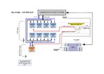
This is a block diagram of the new design based on the 1Gb version of the same NOR flash. Please take a look and let me know if you have any suggestions, especially for the extra logic.
Block_Diagram_2nd.jpg

I have also attached the PDF version of the drawing.

Thanks
 

Attachments

  • Schematic_Illustration_Discussion_2nd_1GB.pdf
    41.6 KB · Views: 159

By the way, I forgot to add that this had nothing to do with interfacing with the STM32F4. This has been designed for a certain system and I just wanted to make sure it will be seen by the system as a dual-die device and work flawlessly based on the new design, without any other modifications. I'm sure the A26 signal has been routed to a similar logic internally for the 2Gb devices to select between dies.
 

I just found in the datasheet that the device identifies itself on the host system by a series of CFI values, which makes it impossible to drop it with two discreet 1Gb devices unless the driver on the host system has been modified.
 

Status
Not open for further replies.

Part and Inventory Search

Welcome to EDABoard.com

Sponsor

Back
Top