Continue to Site

[SOLVED] input pair biasing in a sort of differential circuit

Status
Not open for further replies.

engrMunna

Advanced Member level 4
Full Member level 1
Joined
Oct 25, 2010
Messages
106
Helped
6
Reputation
12
Reaction score
5
Trophy points
1,298
Activity points
2,071
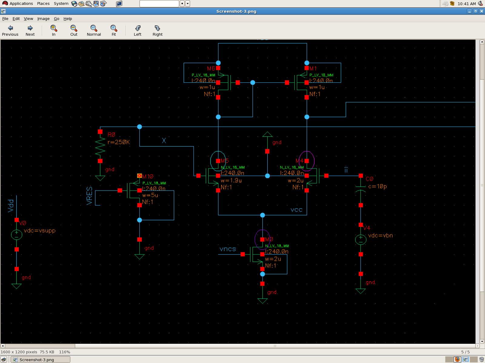
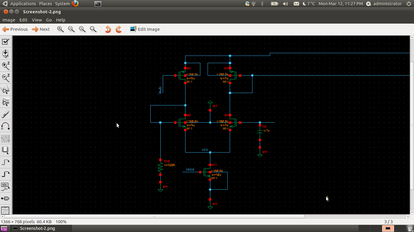
Hi I am using the circuit for current integration. the current input is at the capacitor node. now the thing is that I want to bias it with a tail current of around 8 to 10 uA. But for this tail current to be divided into the two load branches, approximately equally in both the branches, I need some DC biasing at the gate of the input NMOS and the NMOS having the resistor connected to it. But how can I attach a VDC to these gates when this is part of my signal path?
I mean the input NMOS gate will be directly connected to my current input. And thealso there will be some small signal in the feedback of the other NMOS. So how to bias these two THANKS! (NOTE single ended input.)
 

You can use the tail nfet M11 with appropriate bias vncs as constant current source if it works in saturation region. This means the tail voltage vcc is at least about 0.5V. The gate voltages of the differential pair M0,M1 must be at vcc+Vth in order to put the circuit into a reasonable OP. So you would have to connect the bottom nodes of both R10 and C8 to an appropriate bias.

I don't see any feedback from M3 to M6, which is necessary for a diff amplifier. Is this done via isub ?
 

Yeah I am mainly confused about biasing r10 and C8, I mean if I connect the bottom node of C8 to a DC voltage for biasing purpose, how can the gate of M1 be biased due to this becasue won't the capacitor block the DC voltage?
There is no feedback from M3 to M6, this is a current conveyor circuit. isub is a dc voltage source. Please do clarify about biasing the bottom node of C8...thanks!!
 

... how can the gate of M1 be biased due to this becasue won't the capacitor block the DC voltage? ... Please do clarify about biasing the bottom node of C8...thanks!!

Of course a capacitor blocks DC voltage. But think of the S/H method: When the circuit is switched on and the bias voltages are stabilized, the cap is still a "short circuit" (no charge, no voltage between its nodes), so it will "forward" its bottom node voltage (its bias) to the top node, and so to the gate - which puts the circuit into a working OP - if R10 is connected to the same bias. Simulate it!
 

Ok thanks....I will try this tomorrow, and get back to you, as I don't have access to the software right now :). Thanks!
 

Of course a capacitor blocks DC voltage. But think of the S/H method: When the circuit is switched on and the bias voltages are stabilized, the cap is still a "short circuit" (no charge, no voltage between its nodes), so it will "forward" its bottom node voltage (its bias) to the top node, and so to the gate - which puts the circuit into a working OP - if R10 is connected to the same bias. Simulate it!

Hi I tried as you said, like in the attached figure, NMOS M4, I connnected the bottom of the capacitor to the bias value that i need, instead of ground, but it does'nt bias M4. One more way that I found out was to apply the DC bias to the gate of M4 through a very large resistance like 1Gohm, and it works. But from practical point of view, like layout, is this approach feasible?


---------- Post added at 14:34 ---------- Previous post was at 12:47 ----------

Dear erikl, I found a better technique to separate the signal path from the DC bias. Now instead of using the 1G ohm resistance as mentioned in my previous post, I simply replaced the resistor with a PMOS, but the bulk connection of the PMOS is connected to the Drain terminal. this gives a very good control on the pmos resistance through the gate voltage.
 

Ok, fine.
But I think in reality it would work without a resistor or PMOS. You could try it if you add an ic=0 condition to the cap, which is in accordance with reality.
 

I am using the pmos to give the effect of a resistor with a value beyond 700 mega ohm....I havent done a layout yet but it think generating resistances in that region might not be feasible so thats why i am using a pmos. well anyways thanks!
 

Status
Not open for further replies.

Similar threads

Part and Inventory Search

Welcome to EDABoard.com

Sponsor

Back
Top