Continue to Site

Welcome to EDAboard.com

Welcome to our site! EDAboard.com is an international Electronics Discussion Forum focused on EDA software, circuits, schematics, books, theory, papers, asic, pld, 8051, DSP, Network, RF, Analog Design, PCB, Service Manuals... and a whole lot more! To participate you need to register. Registration is free. Click here to register now.

Increase ADC input range

FreshmanNewbie

Advanced Member level 1
Joined
May 10, 2020
Messages
437
Helped
0
Reputation
0
Reaction score
3
Trophy points
18
Activity points
4,333
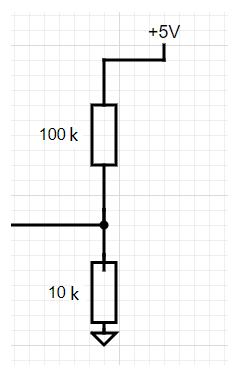
Below is a circuit I have.

1701775173906.png


Initially, I have 2 100k resistors. And the node will be given to an ADC in an MCU. But since the ADC requirement was modified later, the bottom resistor was changed to 10k.

But this increased the sleep current due to the low value resistor. Hence, can you please confirm how to get the voltage with this config (100k & 10k), without modifying the sleep current when it was (100k & 100k)?

I cannot change the footprint now. Please suggest some ideas.
 
Hi,

We see a voltage divider, 10k/100k, GND and +5V. Nothing else.
No ADC, no MCU.
What is this circuit for?

You talk about increasing the ADC input range. What is the ADC input in your schematic? Since the lower node is GND (fixed) and the upper node is +5V (fixed) .... it can only be the center node. But it is also fixed at 5V/11. So what do you want to increase here?

What sleep current are you talking about?
Sleep current usually refers to an MCU? But what MCU exactly?

Maybe you talk about the resistor current, maybe about the increased MCU supply current (crowbar current by not saturated input stage)

Resistor current:
You should be aware about Ohm´s law. Basically the higher the resistor value the lower the current.
But whether this is a good idea or not depends on the required accuracy, precision and the ADC input specifications.
You don´t tell anything about it.

Klaus
 
Depending on MCU input architecture your source Z can impact its accuracy/operation
as well. Klaus's questions very pertinent to getting this right.

Also the R divider network footprint issue ? Resistors, many values in same footprint, explain
why you cant change values again ?


Regards, Dana.
 
Hi,

We see a voltage divider, 10k/100k, GND and +5V. Nothing else.
No ADC, no MCU.
What is this circuit for?

You talk about increasing the ADC input range. What is the ADC input in your schematic? Since the lower node is GND (fixed) and the upper node is +5V (fixed) .... it can only be the center node. But it is also fixed at 5V/11. So what do you want to increase here?

What sleep current are you talking about?
Sleep current usually refers to an MCU? But what MCU exactly?

Maybe you talk about the resistor current, maybe about the increased MCU supply current (crowbar current by not saturated input stage)

Resistor current:
You should be aware about Ohm´s law. Basically the higher the resistor value the lower the current.
But whether this is a good idea or not depends on the required accuracy, precision and the ADC input specifications.
You don´t tell anything about it.

Klaus
Hi,

This is the MCU.

Vcc of MCU = 3.3V

Port of the MCU is RB3 for the ADC Input.

Can you please help with this information?
 
If keeping current consumption through the divider is of prime importance, and we have to assume from the voltages you are measuring the 5V level, the solution is to INCREASE the top resistor value rather than decrease the lower one. Electrically the resulting voltage to the ADC is the same but you should note that the higher impedance it creates will make the ADC more prone to noise and also slow down it's response time. If you are only monitoring a 5V supply level, those might not be critical factors and you might be able to place a capacitor from the ADC input to ground to improve noise rejection.

Allowing for some safety margin if the 5V is slightly higher than it should be, using 150K as the top resistor and 220K as the lower one will give 2.973V to the ADC with 5V applied and give safety margin of 5.6V with current consumption less than about 15uA.

Brian.

Thank you for your answer.

Just a couple of questions from your answer.

1. Can you please explain how increasing the top resistor value will make the ADC more prone to noise and slow down the response time?
2. What can be the value of the capacitor that I can place on the ADC input to ground? Is there any formula or calculation for it?
 
1. Under ideal conditions it would make no difference but in real life, there will be stray signals around, some induced into the wiring and some capacitively or statically coupled to it. With a low value to ground these are 'discharged' more easily so their effect tends to be less. When high value resistors are used there will be less current drained to ground (which is your intention) so influences like those will be more prevalent. As for response time, this is detailed in the data sheet and in Dana's earlier reply. Basically, the ADC doesn't measure 'live' voltages as these could change while the ADC conversion is taking place and produce wrong results. Instead, at the start of the ADC measurement cycle, the voltage on the ADC pin is sampled and held in a capacitor to keep it stable. If the resistance at the input to the ADC is too high, there will be insufficient current to charge the capacitor quickly. This doesn't mean it can't be used, just that you need to use a lower sampling rate to allow time for the voltage to settle before measuring it.

2. Depends on what exactly you are measuring, adding a capacitor and feeding it through high value resistors means it takes even longer to charge and discharge. It will follow the dropped 5V at slower speed. If you are measuring a slow changing voltage there is no problem but if you are trying to measure higher frequencies you have to take into account the time constant of the R and C combination. It is this slowing of the voltage change that helps to reduce noise which is generally of a rapidly changing nature. There is a plus to this, the charge on the extra capacitor helps the ADC to draw input current more quickly so faster conversion rates can be used. The optimal value depends on how quickly the 5V is expected to change, if speed isn't an issue, I would suggest 1nF as a good starting point but make sure it has short connections to the ADC input pin and the VSS pin.

Brian.
 
Below is a circuit I have.

View attachment 186693

Initially, I have 2 100k resistors. And the node will be given to an ADC in an MCU. But since the ADC requirement was modified later, the bottom resistor was changed to 10k.

But this increased the sleep current due to the low value resistor. Hence, can you please confirm how to get the voltage with this config (100k & 10k), without modifying the sleep current when it was (100k & 100k)?

I cannot change the footprint now. Please suggest some ideas.
I suggest you learn to refine your requirements to communicate clearly in engineering terms.

1. Purpose: (function and environment)
2. All inputs
3 All outputs , e.g. ADC Voltage range (= Vref)
4. Show existing hardware and limitations, protection
5. Questions ( like how to scale voltage yet minimize sleep current such as using an active switch.)
 
insufficient info on your design specs for power, source range , ADC range , source impedance requirements.
Below is a circuit I have.

View attachment 186693

Initially, I have 2 100k resistors. And the node will be given to an ADC in an MCU. But since the ADC requirement was modified later, the bottom resistor was changed to 10k.

But this increased the sleep current due to the low value resistor. Hence, can you please confirm how to get the voltage with this config (100k & 10k), without modifying the sleep current when it was (100k & 100k)?

I cannot change the footprint now. Please suggest some ideas.
ureure
 

LaTeX Commands Quick-Menu:

Part and Inventory Search

Welcome to EDABoard.com

Sponsor

Back
Top