perado
Full Member level 2

Hi
1-can anyone explain for me in details, that how bootstraping in second circuit diagram of inverter circuit improve the performance of it compare to first circuit??
2-how it is possible to make a nand gate with the second inverter circuit (just with p-channel transistor)??
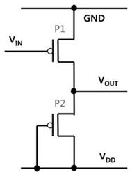
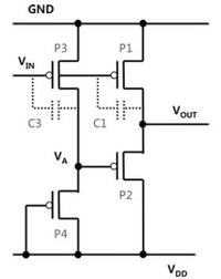
1-can anyone explain for me in details, that how bootstraping in second circuit diagram of inverter circuit improve the performance of it compare to first circuit??
2-how it is possible to make a nand gate with the second inverter circuit (just with p-channel transistor)??


