Continue to Site

Welcome to EDAboard.com

Welcome to our site! EDAboard.com is an international Electronics Discussion Forum focused on EDA software, circuits, schematics, books, theory, papers, asic, pld, 8051, DSP, Network, RF, Analog Design, PCB, Service Manuals... and a whole lot more! To participate you need to register. Registration is free. Click here to register now.

Implementation of Operational Transconductance Amplifier in LTSpice

Status
Not open for further replies.

robi10101298

Junior Member level 2
Joined
May 7, 2020
Messages
20
Helped
0
Reputation
0
Reaction score
0
Trophy points
1
Visit site
Activity points
117
Hello, I need to implement the following circuit in LTSpice but I don't know what VCM, Vg,VCC and C infinite are :(...Can you help me with the symbols for it? Also, the scheme implemented by me it's ok? Thanks!
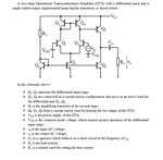
96234628_10213667725885840_7038115341192396800_n.jpg
96780433_10213668503465279_620597356655542272_o.jpg

- - - Updated - - -

I don't know who's R2...VCC= 10V;VCM = 1.5V;vg is a sine wave with a frequency of 1 kH, R1 it's 15k..I need to: a)Calculate the theoretical expressions of the DC collector currents of bipolar transistors Q1–Q8, considering VBE≈ 0.6V. Calculate the theoretical expression of the small-signal voltage gain Av= vo/vg. b)choose a value for R2 and C∞) in order to have a(theoretical)gain value Av= 1500.
 

C∞ admits AC to the load while blocking DC. It's common in audio amplifiers. Farad value can be a wide range. The idea is for it to offer little impedance to your frequency of 1kHz, as compared to the load.

Your other values are reasonable.

- - - Updated - - -

To make your output stage function properly, bias Q5 and Q8 so that one transistor is off as the other conducts, back and forth.

OK, so what values should I choose for R2, C∞ in order to have a(theoretical)gain value Av= 1500?

- - - Updated - - -

This is my final scheme:
96490086_10213674965226819_966358695183122432_o.jpg
 

For C = inf, you may just use "1". That is, 1 F. However, if you see that there are problems with the simulation, just start with e.g. 100 uF and then increase it to 1 mF, 10 mF, 100 mF and see wheter your curves are fine.

For 1.500 V/V gain I would need to calculate a little bit, but you may take the same approach. Just start with any R, e.g. 1k and then increase it or decrease accordingly, e.g.: 1k -> 10k -> 100k -> 1M -> 10M.
 

In addition to an "infinite" capacitor, the simulation needs also an initial condition to bias the output node to a defined DC level. It would be simpler to use a DC source in place of the capacitor.
 

Well, I'm new in this area, I don't think I got your answer...I have some values however: VCC=10V ,VCM=1.5V, R1=15kΩ, Vg is a sine wave with a frequency of 1 kHz, whose amplitude will be chosen so as to ensure minimal distortion of the output signal (i.e. v0 should also be a sine wave); I need to choose a value for R2 and Cinf in order to have a (theoretical)gain value Av=1500, how can I do this?? I'm new in this area and I would like some formulas and tips how can I solve this
 

Your op amp is constructed from portions that do various functions. It would help if you simulate these sections by themselves. Get familiar with how they operate. (For instance, gain may come from two or more sections.)

* long tail pair (differential detector)

* current mirror

* current source (or current limiter)

* common-mode signal rejection

* half-bridge (P-device at top as compared to N-device at top)

* biasing network

* capacitor value determines its impedance to a given AC frequency
 

Well, I'm new in this area, I don't think I got your answer...I have some values however: VCC=10V ,VCM=1.5V, R1=15kΩ, Vg is a sine wave with a frequency of 1 kHz, whose amplitude will be chosen so as to ensure minimal distortion of the output signal (i.e. v0 should also be a sine wave); I need to choose a value for R2 and Cinf in order to have a (theoretical)gain value Av=1500, how can I do this?? I'm new in this area and I would like some formulas and tips how can I solve this

What you do not understand in the following :) :
For C = inf, you may just use "1". That is, 1 F. However, if you see that there are problems with the simulation, just start with e.g. 100 uF and then increase it to 1 mF, 10 mF, 100 mF and see wheter your curves are fine.

For 1.500 V/V gain I would need to calculate a little bit, but you may take the same approach. Just start with any R, e.g. 1k and then increase it or decrease accordingly, e.g.: 1k -> 10k -> 100k -> 1M -> 10M.

Plead tell me so I could help. :)

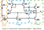
You have the basic, simple opamp class A:

opamp.png

Source: https://payhip.com/b/5Srt ("Preview" button in top right corner).

You just use BJT transistors. Just look for sources that can explain you the basics of opamps. Books as Razavi or Baker in MOS design should help. Once you get the concept of basic opamp structure it will be easier for you.

Please tell me how can I help you.
 
Last edited:

Thanks for your help! What I found is that ICq5=ICq6=ICq7=ICq8=(Vcc - Vbe)/R2; ICq1=ICq2 = [ICq7 / 2 ] * [Beta/(Beta+1)]; ICq4=iCq2-current of Q5; ICq3=ICq1-current of Q3-current of Q4; Beta in my case it's 182.1 because I'm using an BC847A transistor.
A=Vo/Vg = Gm_q2 * Beta_q5 * R1
Gm_q2=ICq2 / Vt that it's aprox 40*ICq2
Did I did something wrong here?
 

Hard to say for me, as the last time I used BJT except bandgap was years ago during studies. I would need some time to verify your calculations. Just try to run simulation and verify them.

If there is anything else I could help you, please write. :)
 
Last edited:

schema.PNG
This is my final scheme...My problem is that when I try to simulate it I get a straight line, do you know why and what can be the cause?
 

Show us your "straight line", that is, the simulation results.
 

Status
Not open for further replies.

Part and Inventory Search

Welcome to EDABoard.com

Sponsor

Back
Top