Continue to Site

Welcome to EDAboard.com

Welcome to our site! EDAboard.com is an international Electronics Discussion Forum focused on EDA software, circuits, schematics, books, theory, papers, asic, pld, 8051, DSP, Network, RF, Analog Design, PCB, Service Manuals... and a whole lot more! To participate you need to register. Registration is free. Click here to register now.

impedance of a return path question

yefj

Advanced Member level 5
Joined
Sep 12, 2019
Messages
1,505
Helped
1
Reputation
2
Reaction score
5
Trophy points
38
Activity points
9,114
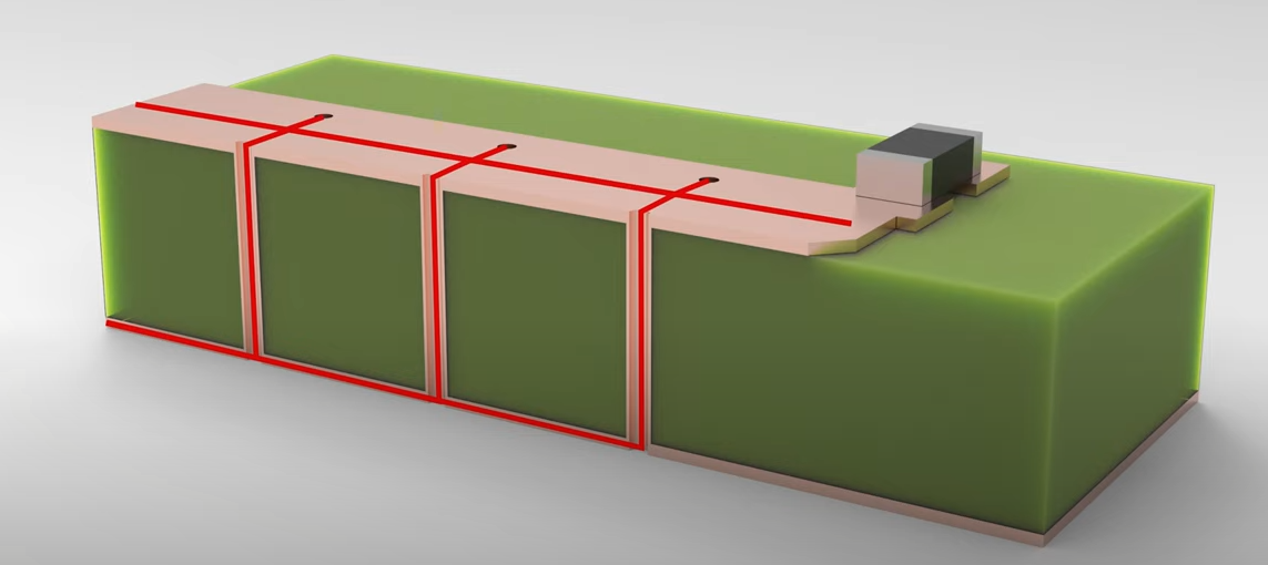
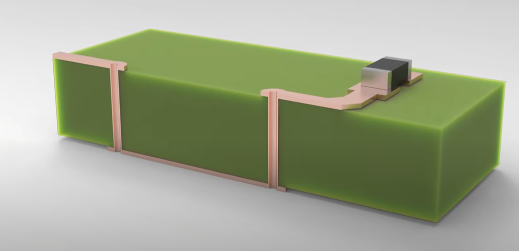
Hello, i am watching this video.they say that the first phot is high impedance whereas the second photo is low impedance.
What exactly makes the impedance high in the first case?
Thanks.
High impedance:
1710145215613.png


Low impedance:

1710145375721.png
 
Hi,

IMHO this video is not really good to explain the inductance of a return path, as indicated in the link. Here, the "input" trace is missing, and consecently the area spanned by the loop and the overall inductance, see [1].

If considering the the trace alone, you can check [2], chapter 8 starting on page 150, to calculate the self-inductance of the trace for a given geometry. Further, you can have a look on a design toolkit [3] to estimate the inductance of the VIAs. Below you can see an example picture, highligthing the inductance in green.

For the two examples, the first one would have a large (self) inductance as the trace itself is long and narrow (at least what is shown) and there are two VIAs with their corresponding inductance. The second one has a lower inductance, but mainly due to the non-interrupted TOP trace. Here, it highly depends on the signal frequency as well as the location of the "input" trace, to judge where the return path is flowing. For "higher" freuencies, the return current will chose the path with the lowest inductance, which is typically in the vicinity of the "input" trace, typically GND plane below the trace to span a small over all loop/area.

1710282953129.png


[1] https://en.wikipedia.org/wiki/Inductance#Inductance_of_a_solenoid
[2] https://nvlpubs.nist.gov/nistpubs/bulletin/08/nbsbulletinv8n1p1_A2b.pdf
[3] https://saturnpcb.com/saturn-pcb-toolkit/

BR
 

LaTeX Commands Quick-Menu:

Part and Inventory Search

Welcome to EDABoard.com

Sponsor

Back
Top