Continue to Site

Welcome to EDAboard.com

Welcome to our site! EDAboard.com is an international Electronics Discussion Forum focused on EDA software, circuits, schematics, books, theory, papers, asic, pld, 8051, DSP, Network, RF, Analog Design, PCB, Service Manuals... and a whole lot more! To participate you need to register. Registration is free. Click here to register now.

[SOLVED] IGBT single low-side with a IR2110 driver. Problem to drive the gate

Status
Not open for further replies.

Noob_tronic

Newbie level 4
Newbie level 4
Joined
Aug 8, 2018
Messages
7
Helped
1
Reputation
2
Reaction score
1
Trophy points
3
Activity points
166
Hello,

To attain a good understanding of necessaries knowledges to drive IGBT and Mosfets is a goal. This way allows me to upgrade electromechanical skills.

The to do list practical projects consist to make :
- Pure sine wave inverter with a driver piloted with pwm micro controller outputs.
- Drive the speed of an asynchronous machine
- An induction forging
- An IGBT/Mosfet Current-Regulation

For information I’ve electrician certifications, but I really try to be humble with electric shocks and the death risk. We will never be reiterated enough that the Electricity is potentially mortal.

The simple first project that I would like to design is the induction forge, because I suppose it’s easiest to make a circuit with a single IGBT to reduce the risk to burn half bridge transistors. The “single low-side driver” design is the purpose of this post.

To discover IR2110 Mosfet/IGBT driver specifications was an adventure. This blog description looks good : http://archive.is/xzSIY . But for the moment I’haven’t got Mosfet and I use IGBT.

Measurements and tests allow me to understand the “IR2110 driver” basic specifications, with the “single low-side driver” design. “LIN input” take a “5V_30kHz_ 50% duty” signal. “VCC input” has a large variable adjusting range from 10 to 18V, with a fixed value for “VDD input” at 9,05V. That design allow me to create a “LO output” tension between 3V to 6V at 30kHz for “GT50N322A” IGBT.
http://www.datasheets360.com/pdf/-6226261397393676843

Unless if I mistaken “LO output” is the threshold/VGE tension which drives the IGBT ON/OFF. To limit IGBT explosion risks, and also try to regulate the current, I made the choice to connect an 40ohm oven resistor with 325V DC “between +circuit and the IGBT collector”. With that design the short circuit with a potential semiconductor explosion should be limited.

When I connected the “GT50N322A” nothing was working ; I suppose that the current driver wasn’t enough to switch this IGBT. I also asked myself about the necessity to connect a diode between emitter/collector and maybe a capacitor ? Unfortunately, I maybe destroyed the ninth IGBT, which was the second to last ; but I don’t know ?

Then I tried to drive the last IGBT with just the “PMW microcontroller output” and an “optocopler TLP521-2”. When I passed 5.5V_30kHz_50%_duty on the gate, the IGBT was conducting 8Amp, but it wasn’t possible to cut off the circuit. A 10kohms resistor was connected between the “Gate and the Emitter”, and a diode between “Emitter and Collector”. I used a 10ohms resistor between the “optocopler output” and the “IGBT gate”.

My questions :
- To plug a MKP capacitor between Emitter and Collector as the “AV R76 MKP” 100nF is maybe the solution ?
- What the difference between a Mosfet drive and an IGBT control ?
- How we can control current in the IGBT ? A current limitation on the gate, or, a VGE tension regulation ?
- Why the data-sheet specification precises VGE tension between 3V and 6V, unless if the Ic(A) f (VGE) curves allow between 7 and 8V ?
- Did I destroyed all this expensives IGBT ?

Thank you for your time and answers.

Nico
:-?

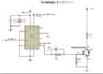
Using the IR2110 as a single low-side driver from tahmidmc.blogspot.com
6737803ed5045ce1324509b64eb98d08ed983f7c.png

IR2110 Logic "1" Input Threshold vs VDD
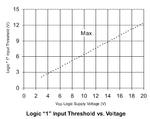
04 - VDD vs in.png
 

in your schematic there is no LOAD on drain of the IGBT !it is dangereous test ! you must haveat least load resistance

- - - Updated - - -

- What the difference between a Mosfet drive and an IGBT control ?
there is not much differences they are similar
 

Thank you Hamid,

Yes you right, it’s dangerous tests as I already precised in the previous post.

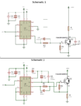
Below attached modifications on schematics with the requested 47Ω load. What is the better solution, schematic 1 or 2 ? Is it acceptable schematics ?

My questions :
A - To plug a MKP capacitor between Emitter and Collector as the “AV R76 MKP” 100nF is maybe the solution ?
B - How we can control current in the IGBT ? A current limitation on the gate, or, a VGE tension regulation ? How can I regulate the current ; is it possible ?
C - Why the data-sheet specification precises VGE tension between 3V and 6V, unless if the Ic(A) f (VGE) curves allow between 7 and 8V and on an another line of the data-sheet appear +-15V ? What is the good PMW tension on the gate ?
D - The 1 kΩ gate resistor isn't maybe the good value ; 10 kΩ is maybe better ?

Thank you for your time and your patience with a noob electronician, but maybe I didn’t post in the good forum ?

Have a nice day

Nicolas

Shematic_1_2.png
 

An IGBT is usually not operated in linear mode, respectively you don't intentionally apply a voltage near the gate threshold of 3 to 6 V. You want a fast transition between on and off state. IR2110 is intended for switch mode operation only.

If you have a special application that involves linear operation of a MOSFET or IGBT, e.g. as a current source, you'll use a different driver. Linear operation however corresponds to large IGBT power dissipation.
 

Thank you FvM,

As precised, I would like to use the IGBT for forge/cooktop applications in frequencies range between 30kHz to 200kHz.

IGBT FGA250N120ANTD is designed for frequencies from 30kHz to 1MHz and should answer to my needs.

Because that looks easiest for the moment, I guess the IR2110 in a single high-voltage high-side driver configuration should answer to first steps with a resistor load.

The resistor charge was used for tests at 30kHz, to limit short circuit risks and to find the good adjustment for that range of frequencies on the gate.

But unfortunately, I guess something wrong because with diferents IGBT and several times when I passed 5.5V gate tension, the IGBT stay on ON without Off state when the gate stop the PMW signal. That the reason why I ask questions on the forum as newbie newcomer. Maybe something wrong with my questions about schematics 1 & 2 attached ?

A - To plug a MKP capacitor between Emitter and Collector as the “AV R76 MKP” 100nF is maybe the solution ?
B - How we can control current in the IGBT ? A current limitation on the gate, or, a VGE tension regulation ? How can I regulate the current ; is it possible ?
C - Why the data-sheet specification precises VGE tension between 3V and 6V, unless if the Ic(A) f (VGE) curves allow between 7 and 8V and on an another line of the data-sheet appear +-15V ? What is the good PMW tension on the gate ?
D - The 1 kΩ gate resistor isn't maybe the good value ; 10 kΩ is maybe better ?


Certainly you’re strong performers in your electronic engineering specialities, well done , but I don’t understand your answers, because I’m a beginner in electronic : my forum name is Noob_tronic...

You’re excessive masteries for me on www.edaboard.com sorry. Thank you for your precious time.

That’s was a pleasure to exchange with you.

Thank you

Shematic_1_2.png
 

Hi,

Schematic1:
You did not supply the high side bootstrap circuit. But the IR2110 has undervoltage detection. I'm not sure whether the high side undervoltage situation affects the low side operation...
Thus I recommend to try to properly supply the high side.

*******
In post#1 you say VDD = 9V, but your pictures show 5V.
--> be sure to use 5V

*******
I don't recommend to use schematic2.

*******
Read datasheets especially regarding PCB layout. Don't use discrete wiring, don't use a vero board, don't use a breadboard.
Take care about minimum creepage and clearance distances.
*******

I recommend to use 10k R_GE instead of 1k.

V_GE should be almost equal to 0V / 12V. Expect less than 0.3V of voltage drop. (Schematic1)


Klaus
 

A - To plug a MKP capacitor between Emitter and Collector as the “AV R76 MKP” 100nF is maybe the solution ?
A capacitor can make sense in resonant circuits. It's useless respectively dangerous for the IGBT in hard switching circuits.

B - How we can control current in the IGBT ? A current limitation on the gate, or, a VGE tension regulation ? How can I regulate the current ; is it possible ?
The current in switching circuits is controlled by varying the load, power supply and duty cycle, it can't be controlled by gate voltage.
C - Why the data-sheet specification precises VGE tension between 3V and 6V, unless if the Ic(A) f (VGE) curves allow between 7 and 8V and on an another line of the data-sheet appear +-15V ? What is the good PMW tension on the gate ?
IGBT in switching applications use either unipolar (e.g. 0/+12 to +15) or bipolar (+/-12 to +/-15) gate voltage, depending on the IGBT specification and driver capabilities. IR2110 isn't well suited for bipolar drive.
Applying a gate voltage that turns the IGBT not fully on or off in a high power application will usually destroy the device within milliseconds.

D - The 1 kΩ gate resistor isn't maybe the good value ; 10 kΩ is maybe better ?
The gate pull-down resistor has no effect as long as the gate driver is powered.
 
  • Like
Reactions: burai

    burai

    Points: 2
    Helpful Answer Positive Rating
Great super answers,

Thank you for your experience, your time and your good teaching skills.

Finally I open an other post and I have to do upgrades, because I’m an impatient newbie.

Attached the schematic 1, which was the solution adopted with modifications requested.

The project goal is to valid a DIY cooktop before to make a prototype forge with litz wires.

Specifications :
300V DC tension
Current regulation
PMW drive with a STM32 or an 32u4 uC

An optocopler between the uC and the IR2110 should be necessary : the TLP521-2 can switch with 50mA uC outputs : https://www.futurlec.com/Datasheet/LED/TLP521.pdf

Use the 32u4 uC with 2 synchronizes timers in order to obtain 2 couples of outputs which can generated the 25mA*2=50mA requested for the TLP521-2, should allow a proper command switch. Or I can use a transistor between the Uc outputs and the optocoupler.

Unless if I mistaken the IR2110 driver just requests a logic level of 5V on the Hin and Lin inputs. So I guess it’s necessary to use approximatively 100kΩ between TLP521-2 outputs and Hin and Lin ?

My questions :
- What is the name of the freeware uses under Ubuntu for that model of schematic ? Fritzing is good for PCB but less precise for post schematics. Gimp modifications aren’t really easy.
- 100kΩ between TLP521-2 outputs and Hin and Lin is the good resistor ?

My to do list skills to upgrade :
- how to regulate the current in a " single inverter high frequency switch " DIY, with a " load current reference " , which should to adjust the frequency, in line with the " current instruction " give to the uC from the user.
- measure easily an inductive load : https://www.electronoobs.com/eng_arduino_tut10_3.php

Thank you for your appreciate help,

If you prefer I can switch to the other post.

Kind regards

Nicolas

Shematic_1_A.png
 

What is the name of the freeware uses under Ubuntu for that model of schematic
I use Kicad for schematics through to PCB layout. It isn't the program used to produce your schematic but the result is similar. It's free and should be in the Ubuntu repository.

Brian.
 

Single low-side IR2110 “NPT” driver ; Gate no switch off, after first switch ; IC=8A

Thank you Betwix and FvM for your advices,

After destroyed 6 chips this Sunday, I decided to install Kicad on my computer. That seems to be an amazing program for electronic schematics.

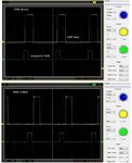
The good new is that my new Hantek USB oscilloscope is working. Attached the arduino PMW outputs signal and the IGBT gate signal without load, about the schematic attached.

The IGBT isn’t plugged during the oscilloscope measures, because the differential circuit breaker cutted off a part of the house network when I tried to do measures in High Voltage. Plug the hantek USB on a laptop without electrical network connexions could be a necessary transition.

Then I will found the way to compile and install the Hantek Debian program on the laptop… 50$ it isn’t expensive for an oscilloscope, but the ubuntu installation isn’t really easy. For the moment Vista allow me to do measure easily on an old school computer.

The next step of tests is to replace the load with a cooktop induction self with capacitors in parallel. Finally I should used a "litz forge".

Simple transition measures should allow me to understand the method to control an IGBT with a driver.

About schematics, the frequency on the gate is 30kHz, and the voltage is almost 15V. But a new time the gate refused to cutt off after the first switch. I don’t understand. Could you please help to know what’s wrong with my schematic please. Maybe the 30 kHz frequency isn’t good ?

The worst in that story is that I reached the goal one time, with a basic optocopler, bu t I can’t found a second time the same schematic… But that the occasion to use a driver for a future half bridge schematic.

Kind regards

Nicolas

References :
FGA25N120ANTD
http://www.farnell.com/datasheets/1774719.pdf
IR2110
http://www.infineon.com/dgdl/ir2110.pdf?fileId=5546d462533600a4015355c80333167e
http://archive.is/xzSIY

Kicad files and pdf schematics
View attachment Files_schematics_kicad_IR2110_FGA25N120ANTD.zip

Print_schematic.jpg
A_Oscilloscope_measures.jpg
 

Attachments

  • A_Print_schematic.pdf
    65.5 KB · Views: 158
Re: Single low-side IR2110 “NPT” driver ; Gate no switch off, after first switch ; IC

differential circuit breaker cutted off a part of the house network when I tried to do measures in High Voltage. Plug the hantek USB on a laptop without electrical network connexions could be a necessary transition.

I guess you have a ground fault interrupter (gfi). Maybe the cause is a ground loop problem. I tried to hook up my laptop computer to the house entertainment system. A loud hum came from the speakers. In order to fix it I had to unplug the laptop power supply. (Either that or unplug incoming cable tv.)

In a similar manner you may need to isolate your laptop from house wiring, when you run the usb oscilloscope.
 

Hi,

Schematics:
* you need two / spiit GND planes.
* you need at least 6mm clearance distance between both low voltage and high voltage circuits.
* every GND pin of every device needs to be connected to the common GND plane.
* every supply pin on every part needs to have a ceramics capacitor with short connection to GND plane.
* don't use series resistors (20k) on IR2110 inputs.
* use pulldown resistors instead. Value needs to be chosen to get fast and clean signals.
* AVR: AVCC, ARef, Reset need to be connected
* SD pin needs to be driven with proper signal levels

Scope pictures:
The delay between AVR_PWM signals and IR2110_output signals should be less than 1us - dominated by the optocoupler delay.

Klaus
 

PC817 is too slow to transmit 30 kHz pwm without pulse width distortion. If at all, it need a well dimensioned load resistor, e.g. 500 ohm to 1k. The present circuit uses only internal IR2110 pull down resistors with at least several 100k, it can hardly transmit > 1 kHz pulse frequencies.


The "47 ohm" load looks still suspicious. Do you actually use a resistor with 2 kW power rating?
 

Thank you Super Moderators,

Sorry for the last post which wasn’t described precisely my main question. From your opinion :
“ why the gate isn’t switch off ? What is the destroyer physical phenomena ? “

After KlausST answer, I’m betting on the ceramic capacitor, but ….

Maybe BradTheRad from Minneapolis gave me maybe the good " Agile Priority ", with a necessary oscilloscope measure on the gate when the test is under high voltage.

Oscilloscope measures are demonstrated that the signal should be good on the gate. 15V_PMW_30kHz signal which switch off under zero volt should do the job ; that should switch off the NPT IGBT FGA25N120ANTD. Because I can’t measure on high voltage the gate state evolution with my USB oscilloscope, I’m disappointed.

KlausST, thank you for your to do list/suggestions :
* The GND are splitted between the 5V USB 328p micro-controller with the optocopler and the other part of the schematic. As you know that limits harmonics and interferences on the microcontroller. But maybe I don't understand something ?
* About ceramic capacitors, from my opinion that maybe the only reason why it’s not switching properly ; I’ll equipped all power supplies inputs as the VDD 5V model.
* The Lin IR2110 will been equipped with a pull down resistor.
* I never connected the reset or the AVR microcontroller, and that works. Is it my priority ?
* The SD switch is making the job with a proper IR2110 cutt off, if I believe the oscilloscope IGBT gate signal

Than you FvM :
* That’s true, the PC 817 is giving a dirty signal output, but IR2110 op-amps are doing a great filter job. As you can see the signal output is almost clean on the IGBT gate. IR2110 specifications is IO+/- 2A, that means that the output signal can deliver and cut off 2A, isn’t it ?
* About the current limitation and your previous answer, when I will been capable to switch off the IGBT at 30kHz, do you think that could be possible to do a current limitation range on the IR2110 VCC, which can maybe limit the gate current and the current load ?
* On the https://www.nxp.com/docs/en/application-note/AN5030.pdf IGBT is controlled with 0/+18V ; do you think it’s possible to drive the gate with 15V, or that’s maybe the reason why it’s not switching properly.

Kind regards

Nicolas

View attachment Files_schematics_kicad_IR2110_FGA25N120ANTD.zip
View attachment A_Print_schematic.pdf
A_Oscilloscope_measures.jpg
 

IGBT driver, problem to drive the gate. Super Moderator censure on www.edaboard.com ?

Hello,

The post moderator refused to validate the last erratum with the good attached file.

Indeed, the subject reason invocate is :
Reason: *Duplicate post while awaiting moderator*

But I changed the attached files and the text with a new schematic which was integrated the 10 kΩ gate resistor forgot. Without that modification I felt stupid, sorry for this mistake.

How we can signal the problem to a www.edaboard.com Big Boss Moderator please, because that situation are maybe exceeding a nice newbie hazing. That discredits me. Few answers can be considered as mockingly and disrespectful.

Attached the previous schematic already post this morning but censured.

Finally this "post censured" isn’t allowing me to have an answer to my simple question :

Why the gate refused to switch off. That destroyed the NPT IGBT with a continuous 8A _ 320Vdc power ?


I maybe destroyed 20 IGBT during measures.

Respectfully

Nicolas

NB : a big thank you to passionate volunteers, who really try to help newbies and who knows who they are
Sorry to complain

View attachment A_Print_schematic_Va.pdf
A_Oscilloscope_measures.jpg
 

Finally this "post censured" isn’t allowing me to have an answer to my simple question :
Nothing is censored here, just multiple copies of the same post "filtered". I see some pictures copied again and again. Please try to focus on new information.

- - - Updated - - -

If you want to correct a circuit detail, post just the new schematic with a short explanation, don't repeat all the other stuff not related to the modification.

It took more than ten days until you finally mentioned that you have destroyed multiple IGBT with your test setup. I doubt however that we have seen yet the real schematic. It's effectively impossible to get the shown gate waveform when driving IR2110 with PC817 and no LIN pull-down. The suspected missing gate pull-down is however almost useless.

It may be the case that you are misunderstanding the cause for IGBT damage. Switching large output currents can have all kinds of unexpected effects in a not properly layouted circuit, e.g. parasitic oscillations that quickly destroy an IGBT.

- - - Updated - - -

To consider the shown gate waveform as thrustworthy, it should be reproducable over a wide duty cycle range, e.g. 5 to 50 %. Is this the case?
 

Status
Not open for further replies.

Part and Inventory Search

Welcome to EDABoard.com

Sponsor

Back
Top