GuiRitter
Junior Member level 1

- Joined
- Oct 19, 2011
- Messages
- 17
- Helped
- 0
- Reputation
- 0
- Reaction score
- 0
- Trophy points
- 1,281
- Activity points
- 1,560
Hi everyone.
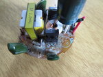
I like to open compact fluorescent lamps that don't work anymore to scavenge components from the ballast (and many other products). In the last one that I opened, I saw some kind or dirt or damage that doesn't seem to come from any component. Here's what it looks like (4000×3000 version in the attachments):

I did nothing with it after removing it from the lamp, except moving two capacitors to show the area better. The color of the component markers ("Top silk" in Proteus ARES) is like that for the entire board. On the bottom side, almost no sign of dirt/damage, so I didn't bothered with a photo.
Someone have an idea of what it could be? More importantly, is it safe to handle this board and remove its components?
Thanks in advance.
I like to open compact fluorescent lamps that don't work anymore to scavenge components from the ballast (and many other products). In the last one that I opened, I saw some kind or dirt or damage that doesn't seem to come from any component. Here's what it looks like (4000×3000 version in the attachments):

I did nothing with it after removing it from the lamp, except moving two capacitors to show the area better. The color of the component markers ("Top silk" in Proteus ARES) is like that for the entire board. On the bottom side, almost no sign of dirt/damage, so I didn't bothered with a photo.
Someone have an idea of what it could be? More importantly, is it safe to handle this board and remove its components?
Thanks in advance.


