Continue to Site

Welcome to EDAboard.com

Welcome to our site! EDAboard.com is an international Electronics Discussion Forum focused on EDA software, circuits, schematics, books, theory, papers, asic, pld, 8051, DSP, Network, RF, Analog Design, PCB, Service Manuals... and a whole lot more! To participate you need to register. Registration is free. Click here to register now.

I2C interface protection, Anyone put values on components for me?

Status
Not open for further replies.

Calltronics

Newbie
Newbie level 2
Joined
May 7, 2023
Messages
2
Helped
0
Reputation
0
Reaction score
0
Trophy points
1
Activity points
13
I have to reverse engineer this interface to the microchip memory.
Anyone shed anylight on the value of the Zener.
Also the capacitors.

Appreciate your help
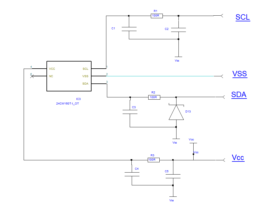

1683450109167.png
 

The protection circuit looks completely arbitary. Why a zener at SDA, why not at SCL or VCC?
Capacitors at SDA and SCL have to be small (maximal 10 pF range) and don't actually provide releavant protection, e.g. against ESD. At best they cut RF interferences, e.g. if the board ist placed near a GSM antenna. I2C data rate and SDA pull-up values have to be known. Vcc filters can use 100 nF up to uF range without problems.

Generally speaking, the chip may either need no protection at all or more effective protection, depending on the application enviroment. The fact that you see this circuit in a product doesn't necessarily imply that it's well considered or even serves a purpose.
 

Spec on chip :

1685183505890.png


This spec seems to allow the internal protection diodes to conduct which is not advisable,
so I would clamp at Vin <= Vcc + .7. So worst case a zener value for that.

Protection considerations :


Be aware that LV zeners can add a lot of C to the buss, compromising timing at the higher
speeds. So choose carefully.


Regards, Dana.
 

Status
Not open for further replies.

Similar threads

Part and Inventory Search

Welcome to EDABoard.com

Sponsor

Back
Top