dressler6
Newbie level 6

Hi. all~
It is about stb simulation and AC simulation of Specter.
There is buffer composed of 2 stage OTA.
- DC gain 60dB
- 0dB Freq.=1Meg
- PM=60'
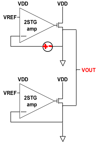
If these two buffers are composed as shown in Fig.1 and frequency stability is evaluated, the loop gain using STB method is 0dB. However, VOUT is almost VREF.
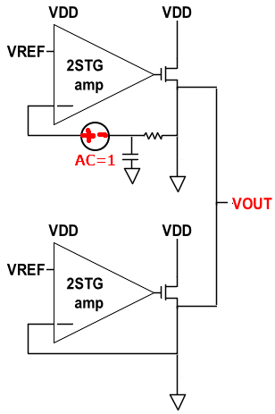
In Fig.2 the loop gain using RC filter method (with AC=1) becomes about 20dB. However, VOUT is also almost VREF.
(Discussion of frequency stability is excluded.)
Please explain why these results were obtained.

[Figure 1]

[Figure 2]
It is about stb simulation and AC simulation of Specter.
There is buffer composed of 2 stage OTA.
- DC gain 60dB
- 0dB Freq.=1Meg
- PM=60'
If these two buffers are composed as shown in Fig.1 and frequency stability is evaluated, the loop gain using STB method is 0dB. However, VOUT is almost VREF.
In Fig.2 the loop gain using RC filter method (with AC=1) becomes about 20dB. However, VOUT is also almost VREF.
(Discussion of frequency stability is excluded.)
Please explain why these results were obtained.
[Figure 1]
[Figure 2]


