Continue to Site

Welcome to EDAboard.com

Welcome to our site! EDAboard.com is an international Electronics Discussion Forum focused on EDA software, circuits, schematics, books, theory, papers, asic, pld, 8051, DSP, Network, RF, Analog Design, PCB, Service Manuals... and a whole lot more! To participate you need to register. Registration is free. Click here to register now.

[SOLVED] How to simulate a circuit with feedback with a test voltage after making a breakpoint

Status
Not open for further replies.

rmanalo

Advanced Member level 4
Full Member level 1
Joined
Feb 8, 2017
Messages
107
Helped
16
Reputation
32
Reaction score
16
Trophy points
18
Location
Philippines
Activity points
979
Hello everyone, there's a circuit that is in feedback that I believe is not one of the 4 feedback topologies. I'd like to simulate the feedback loop by putting a break point and inserting a test voltage, Vt, and get the output voltage Vo and measure the feedback loop, Vo/Vt. as seen in the attached figure as an example.
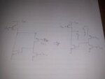
54524773_337434966910385_3739758544388358144_n.jpg

However, if put a break point, would that mean that I need an appropriate value for Vt for the the circuit to function properly (as if the break point didn't exist in the first place)? What are your comments in this method?
 

You must break the loop at a point where the load is rather large (e.g. at the gate input) - otherwise the loop gain is not correct (because the load is present under closed-loop conditions).
More than that. the breaking must not change the normal DC operating point.
 
A better breaking point would be at the gate of the NMOS in the left branch of your circuit. Of course, the type of the feedback will depend on where you take your output from, which you don't show in your drawing, but assuming it is between the drains of the PMOS and NMOS in the folded branch (right branch in your drawing), then you can consider it as shunt-series, that is shunt at the output and series at the input.

Anyway, you can insert a voltage source in series at the break point. The side of the v.source facing the gate of the left branch NMOS is the input stimulus and the return voltage is the voltage at the other side of the v.source - both with respect to ground. Take the ratio and that's your loop gain, at least for low frequencies. This is part of the Middlebrook's method for testing stability.
If you're using cadence, best to break the loop with an iprobe and do stb analysis.
 
You must break the loop at a point where the load is rather large (e.g. at the gate input) - otherwise the loop gain is not correct (because the load is present under closed-loop conditions).

Yes I realized this a while later. In this situation, would it be a good idea to replace the test voltage, Vt, to a test current, It, for a low input impedace such as the source of the PMOS transistor?

More than that. the breaking must not change the normal DC operating point.
This is what I meant when I said "an appropriate value for Vt", should the DC value for Vt be the normal operating value of the node before breaking the loop?
Here were my steps:
1. Simulate the complete circuit and find the node voltages or branch currents.
2. Break the loop at the gate (or source) and add a test voltage (or current) with a DC value of the node voltage (or branch current).
3. Add an AC signal to Vt (or It) and plot Vo/Vt (or Vo/It).

Thoughts on this procedure?
 

Here are two acceptable methods of simulating the loop gain (approx results at high frequencies) that will keep the dc operating point intact but will give you the loop gain T. In the first case, your stimulus faces very big impedance looking into the gate. In the second case your current stimulus faces low impedance (1/gm).

edaboard.PNG
 
In order to ensure that the normal DC operating point does not change, using the node voltages from a previous DC op simulation might not be enough. For example, of your loop gain is 1000 and you set 1V instead of 0.999V you will have a massive error!
Also, you are not capturing the loading effect of the break point (the capacitance at the gate, etc)

The two possible methods are:
1. Have three parallel circuits like shown below. A for DC operating Point, C Loading and B for actual loop gain measurement.
edaboard_middlebrook.jpg

Since this is measuring the loop characteristics with loading and at the correct operating point, this method would be valid always. I.e. There are no assumptions here.

2. If you are using Cadence Virtuoso, use STB analysis. This does the same as above without much effort. :)

PS Not sure why the image is rotated.
 
Actually, stb in cadence doesn't do this thing, in fact, it is very far from this thing.
 
This is the same approach I used a lot for my LDO designs before I knew about the STB analysis.
 

You can read an article called "Striving for small-signal stability". Basically, cadence's iprobe stb measurement uses Middlebrook's method for feedback stability but with some modifications.
 
Status
Not open for further replies.

Part and Inventory Search

Welcome to EDABoard.com

Sponsor

Back
Top