hiii...
thanx for the reply
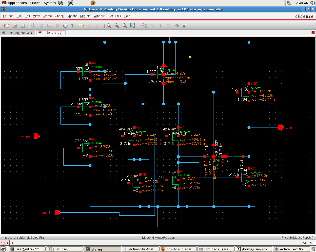
here is an image of the circuit after the simulation along with the operating voltages...

---------- Post added at 07:00 ---------- Previous post was at 06:54 ----------
Hi r@m$
- you are biasing with very small currents, this makes life a whole lot harder, cut yourself some slack and use an ideal current source to bias the first branch, use at least 10uA to begin with, you can always optimize for power later
- show vdsat, so you can verify all devices are in saturation, in particular M10 is probably not
- show gm and gds so you can estimate the gain in each stage
- identify the input common range by running a coarse two-source DC sweep of the two inputs and plotting the output voltage, this will also provide the output common mode
- set both inputs in the middle of the input common range, and run OP, if the output is not saturated (one of the FET in the output branch will not be in saturation in that case) then you need to compensate for input offset
- to adjust for the input offset -if necessary- keep one input in the middle of the input range and run a fine DC sweep on the other and notice the point where the output crosses the middle of its output range (not 0)
- set the two inputs so the output is in the middle of its range
- run OP and AC analysis in this condition
- adjust gm and gds of your devices until you get the desired DC gain and bandwidth
- adjust compensation for decent phase margin