how to run analysis of OP Amp(low power)
- Thread starter r@m$
- Start date
- Status
- Not open for further replies.
NO1_NANO
Newbie level 4

If you want only to do AC analysis, you just have to give the vdd, vss voltages by "vdc source", and add a load capacitance to the output, the voltages of vin+ and vin- can also be given by "vdc source", you only have to give ac values in the right place bisides the dc values.
nassim_el85
Member level 4

For testing such an OTA with differential input and single output, you should know the input and output common-mode voltages for which the OTA is designed for. Also you need to design a test-bench circuit and use this OTA in a feedback loop, which sets the output common-mode voltage of the OTA based on it's input common-mode voltage. For example, if the OTA has equal input and output common-mode voltages, you can use a simple resistive negative feedback from the output of the OTA to its negative input and then apply the input signal to the positive input node of the OTA. The input signal should contain a DC value equal to the common-mode voltage of the amplifier and an ac component.
LvW
Advanced Member level 6

I am getting negative gain of the order -50 dB
but i am supposed to get 75dB
Most probably, the reason is an uncorrect bias point due to the input offset voltage.
Recommendation:
* At first, perform a dc analysis (with µV resolution between +/- 10mV) to determine the necessary input offset.
* Then, apply the corresponding dc voltage together with the ac input.
* As a result, you get the open-loop gain.
nassim_el85
Member level 4
Also: 1- choose the resistance value as large as possible, not to affect on the OTA ac operation. 2- Use a large capacitor from the negative input of the OTA to ground, to zero the ac value of this pin.
DenisMark
Full Member level 6
Hi r@m$.
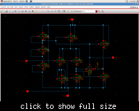
I would like just notice you that in circuit you shown you have a sufficient mistake.
May be you already correct it. If not you have a wrong connection of output terminal.
May be it's a reason of unexpected simulation results.
I would like just notice you that in circuit you shown you have a sufficient mistake.
May be you already correct it. If not you have a wrong connection of output terminal.
May be it's a reason of unexpected simulation results.
nassim_el85
Member level 4
Agree with DenisMark! Follow the signal path!!!
r@m$
Junior Member level 3
hsh22
Newbie level 3
i dont quite understand why the Vout is connecting to that point
---------- Post added at 19:08 ---------- Previous post was at 18:55 ----------
I see the new one.
Are you sure the M2 can get the correct gate voltage Vg2. I just used the poly resistance
---------- Post added at 19:08 ---------- Previous post was at 18:55 ----------
I see the new one.
Are you sure the M2 can get the correct gate voltage Vg2. I just used the poly resistance
LvW
Advanced Member level 6
Hi r@m$,
even after correcting your circuit, my reply#5 ist still valid.
Since you have asked how to determine offset - it is explaine in posting#5 (dc analysis for very small input voltages with very good resolution).
even after correcting your circuit, my reply#5 ist still valid.
Since you have asked how to determine offset - it is explaine in posting#5 (dc analysis for very small input voltages with very good resolution).
LvW
Advanced Member level 6
hiii LvW...
tanx for the reply..
but i dont know how to get the input offset voltage from the dc analysis
The dc analysis gives the transfer characteristic around the operating point - and it crosses the zero-volt line at Voff.
nassim_el85
Member level 4
I can't understand what do you mean by the input offset voltage!! can you explain more? What is the source of this offset?
I still think that after correcting the output node, the description in my first and second replies should be followed.
I still think that after correcting the output node, the description in my first and second replies should be followed.
LvW
Advanced Member level 6
I can't understand what do you mean by the input offset voltage!! can you explain more? What is the source of this offset?
I still think that after correcting the output node, the description in my first and second replies should be followed.
If you work with opamps and are going to design opamps it is important to understand the relevant specifications.
In case of ideal matching of all components the opamp output (split supply assumed) should be zero for zero input voltages.
However, in reality this is not the case. The offset voltage Voff is the voltage that is necessary to apply across the input nodes to produce Vout=0 volts. The dc transfer curve crosses the zero line for a (small) input voltage that is identical to Voff (µVolts for good opamps, mVolts for universal units).
jaxrobinson
Newbie level 5
Add Vcc source to the circuit so that you can run the amplifier.
- Status
- Not open for further replies.
Similar threads
-
How to match power dependent Impedance (large signal)
- Started by ICRF
- Replies: 2
-
[Moved]How to design a Low Pass Filter for low frequency?
- Started by quickanswers
- Replies: 7
-
Slew rate simulation of a discrete Op amp on Ltspice
- Started by PorDeseign00
- Replies: 39
-
Power Switch of Multiple Voltage level
- Started by fredhdx573
- Replies: 9
-
Stability Analysis for Bandgap
- Started by KGF KING
- Replies: 1


