Pulasthi_Perera
Junior Member level 1

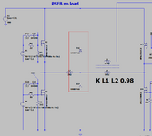
I have been designing and testing a closed loop phase shifted full bridge.
When my Current Reference to the controller is 0A.bridge of the Phase shifted full bridge is switching at 50% with no overlapping. At this moment i observe high EMI induction in the Surroundings because in the Deadtime when one FET is open and other is also open but it Coss is charging to 400V.Now this Coss is resonates with the leakage inductance of the Transformer and produce EMI in the deadtime.
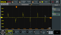
The Transformer primary waveform is attached and you can see the voltage spikes that are coupling to the secondary.
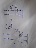
And my understanding of what is happening is drawn in the other attachment.
Can anybody did me on how to solve this issue? how can i Discharge the Coss of MOSFETS without delivering power to the secondary and prevent resonation.I see heavy EMI in this occation enough to make my monitor flicker.
When my Current Reference to the controller is 0A.bridge of the Phase shifted full bridge is switching at 50% with no overlapping. At this moment i observe high EMI induction in the Surroundings because in the Deadtime when one FET is open and other is also open but it Coss is charging to 400V.Now this Coss is resonates with the leakage inductance of the Transformer and produce EMI in the deadtime.
The Transformer primary waveform is attached and you can see the voltage spikes that are coupling to the secondary.
And my understanding of what is happening is drawn in the other attachment.
Can anybody did me on how to solve this issue? how can i Discharge the Coss of MOSFETS without delivering power to the secondary and prevent resonation.I see heavy EMI in this occation enough to make my monitor flicker.