Continue to Site

Welcome to EDAboard.com

Welcome to our site! EDAboard.com is an international Electronics Discussion Forum focused on EDA software, circuits, schematics, books, theory, papers, asic, pld, 8051, DSP, Network, RF, Analog Design, PCB, Service Manuals... and a whole lot more! To participate you need to register. Registration is free. Click here to register now.

How to reduce the input-referred noise current of Regulated Common Gate Transimpedace Amplifier?

Status
Not open for further replies.

melkord

Full Member level 3
Full Member level 3
Joined
May 18, 2018
Messages
151
Helped
0
Reputation
0
Reaction score
1
Trophy points
18
Visit site
Activity points
1,772
Hi, I think it is time to ask for some help regarding this circuit.
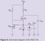
I have this circuit and would like to hear some suggestions on things I can do to reduce the input-referred noise current.
Right now, I can get it around 5-6 pA/sqrt(Hz) with ~400uA,1.8V. I would love to have it below 3, if possible.

Changing gm seems does not work.
So, the suggestion could be any modification of that circuit, while keeping it as common gate.
Other relatively simple topologies with power consumption <~2.0mW(1.8V, ~1200uA, 0.18um) would be as well appreciated.

1608041701651.png
 

Attachments

  • 1608041683575.png
    1608041683575.png
    33.4 KB · Views: 160

Hi,

To reduce input referred noise you should decrese noise or increase gain.
Increasing Gm sounds a good idea for increasing gain, you didn't tell why it doesn't work and how did you try to increase? With increasing bias current or device sizing?
Low frequency noise is the issue (flicker) or high (thermal)?
How much bandwidth you need? Inductive load can be a solution?

BW = 7MHz. I prefer not to use inductive load here.

Sorry, I was not clear enough.
I increased gm by increasing bias current and size(increasing gm/id).
I am expecting the output voltage to be ~1.3V, RL = 10k. in the CG stage, the current is 50uA, gmid=~12.
The current on CS stage is 35uA, gmid=14, and its load is an active load with rout=11k.
The last time I checked, it is a little bit difficult already to increase the current of CS stage while keeping them in saturation.

I am still not getting the intuition about flicker vs thermal, so I cannot answer this question.
THe analytical model that I wrote so far is only considering the thermal noise and it is quite close to the simulation result.

let me know if you need any more information.
 

Hi,

At 7MHz you have to consider that flicker noise is also relevant. I remember when I designed a circuit with ~200uA consumption and its noise corner frequency was in the n*1MHz range. In your case I would simulate AC noise and find where is the corner frequency.
Btw I asked low or high freq only because if you have an issue with flicker noise then you can get better result with PMOS amlifier and you can influence it with gate area (bigger = better) also.
There isn't too much way to decrease thermal noise, I guess you cannot keep the circuit at -40Cdeg, so I think the best way is to increase Gm with bias current and increase its width to keep it in saturation. Strange it didn't work for you.
Maybe an option is if you want to keep the resistor load is you should add PMOS current source in paralel with the load resistor and increase the drain resistance. As I remember it can help, not sure. Check Razavi RF Microelectronics, at the LNA/Mixer design sections, there are good ideas.
And it is not in front of me how the left side transistor and its load contribute to ouput noise exactly, but you should try to filter the gate with a capacitor of Mn.
Finally I think your bandwidth is low enough to browse for active noise canceling too, but unfortunately I cannot help with that.
 

Looking at the schematic I think that your main input referred noise contributors are the bias current Ib and the RD noise current. The bias current source noise is directly at the input. The RD noise current refers to input at almost 1:1 ratio because it is a common gate stage. The CG transistor Mn noise current doesn't contribute noise for low enough frequencies as is the case with all cascode devices. Its noise will appear at high frequencies. I think this is the reason why you don't see effect on noise when you increase gm. At low frequencies the auxiliary amplifier Mnrg and Rrg also don't contribute to input noise
 

Status
Not open for further replies.

Part and Inventory Search

Welcome to EDABoard.com

Sponsor

Back
Top