Continue to Site

Welcome to EDAboard.com

Welcome to our site! EDAboard.com is an international Electronics Discussion Forum focused on EDA software, circuits, schematics, books, theory, papers, asic, pld, 8051, DSP, Network, RF, Analog Design, PCB, Service Manuals... and a whole lot more! To participate you need to register. Registration is free. Click here to register now.

How to modify and optimize this circuit? (current source using FET and OA)

Status
Not open for further replies.

uoficowboy

Full Member level 3
Full Member level 3
Joined
Apr 4, 2009
Messages
169
Helped
6
Reputation
12
Reaction score
5
Trophy points
1,298
Location
Seattle, Wa, USA
Visit site
Activity points
2,964
How to analyze and optimize this circuit? (current source using FET and OA)

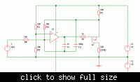
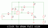
Hi - I want to modify a current source circuit. I've attached a screen capture of the circuit in LTSpice as well as the bode plot of the output (the drain of M1 - though really the output is the current through R2). The current values are mostly just values that I found that produced decent results. The FET was chosen to be wimpy and my hope was that it would have low transconductance (I thought that would help with stability). The OA was chosen to be a fairly general purpose precision OA with fairly normal GBP (1MHz).

The bode plot looks generally like a three pole low pass filter to me (but I could be missing something!) It looks like R4 + C1 gives the first pole [at 1/(2*pi*R4*C1)]. The second pole is from R3 and the Ciss of M1 [again, 1/(2*pi*R3*CissM1)]. The third from the OA.

To optimize this circuit, I'm thinking I'd want to get the first two poles to be at whatever filter function I want (ie choose them to match that of a two pole bessel). And I'd want the pole from the OA to be way past the other two (so as to keep gain high before the cutoff frequency of the first two poles). Does that all make sense? Is there any important relationship between the R4/C1 pole and the R3/M1 pole that I need to be careful of? (ie make sure one is at a lower frequency than the other, or something like that). Any general feelings on how to choose the GBP of my OA? Any other OA parameters I should be concerned about?

As for what I care about from this circuit - I want DC accuracy, stability, ability to handle the voltage on the FET source changing (there will be the equivalent of a AC voltage source between the bottom of R2 and ground in the actual circuit that this is going into) and bandwidth around maybe 1KHz (that part isn't completely nailed down yet). The circuit is for a personal project.

Thanks for your help!!
 

Attachments

  • Current Source With Bode.png
    Current Source With Bode.png
    32.9 KB · Views: 112
  • Current Source.png
    Current Source.png
    33.3 KB · Views: 105
Last edited:

Hi

A fundamental problem with that circuit is that you're driving the load from a MOSFET source, which has a naturally low output impedance. However a current source should have a high output impedance. The opamp tries to correct that, but it will struggle at higher frequencies.

Another issue is that when the output voltage changes, the opamp's output voltage has to change by a similar amount. Again, it will struggle at high frequencies.

Finally, and most importantly, the loop gain of the circuit depends entirely on the load impedance. That means your stability is very load dependent.

I think a better approach would be to use a P channel MOSFET as in the circuit below. Driving the load from the MOSFET source means you have a naturally high output impedance.

All the opamp has to do is set the voltage across R2 equal to the input voltage. It doesn't have to follow any voltage swing on the load, and since there's no direct feedback from the output, stability is easier to achieve, and not strongly affected by the load impedance.

You may still need C1 or C2 (not both) to help with stability, but it should be fairly easy to get good results. When you're checking stability, don't forget to test with reactive loads, especially inductive ones.

Cheers - Godfrey


I agree about the PMOS suggestion. An important advantage of the output transistor connected as source follower is less current dependent gain. For the compensation, I'm pretty sure that C1 should be used rather than C2. The latter doesn't cancel the gate capacitance related pole and may have difficulties to achieve stable behavior at all. C1 should be supplemented by a series resistor, allowing for a better loop characteristic adjustment.
 
Last edited:
The compensation is tricky.

If C1 is used, all we're really doing is reducing the opamp's gain-bandwidth, but the pole due to the MOSFET's gate capacitance is still in the overall feedback loop through R4. If we want to avoid a nasty peak in the response, the unity loop gain frequency needs to be set well below the MOSFET-related pole, which will slow the circuit down significantly.

Using C2 as a speed-up capacitor across R4 is a different story. Here the idea is to create a pole-zero pair close to the unity loop gain frequency, to give some extra phase margin. It's very limited though, contributing a maximum of about 18 degrees. Nevertheless, it can work well if the MOSFET's pole is close to or above the unity loop gain frequency.

Depending on the application, some sort of transitional compensation might be a good compromise. e.g. In the circuit below, the feedback take off point is shifted from the MOSFET source to the opamp output at a fairly low frequency, well below the MOSFET's pole, but the circuit still has fairly high gain above that frequency.


Hi

A fundamental problem with that circuit is that you're driving the load from a MOSFET source, which has a naturally low output impedance. However a current source should have a high output impedance. The opamp tries to correct that, but it will struggle at higher frequencies.

Another issue is that when the output voltage changes, the opamp's output voltage has to change by a similar amount. Again, it will struggle at high frequencies.

Finally, and most importantly, the loop gain of the circuit depends entirely on the load impedance. That means your stability is very load dependent.

I think a better approach would be to use a P channel MOSFET as in the circuit below. Driving the load from the MOSFET source means you have a naturally high output impedance.

All the opamp has to do is set the voltage across R2 equal to the input voltage. It doesn't have to follow any voltage swing on the load, and since there's no direct feedback from the output, stability is easier to achieve, and not strongly affected by the load impedance.

You may still need C1 or C2 (not both) to help with stability, but it should be fairly easy to get good results. When you're checking stability, don't forget to test with reactive loads, especially inductive ones.

Cheers - Godfrey
Hi Godfrey - I can see your point regarding the problem with the OA's output having to follow the output voltage. That makes perfect sense. However, I'm not sure I understand how you would define the output impedance of a current source? Can you clarify that for me please?

I should mention that my load will be a shunt resistor - that will be carrying between 0 and maybe 10A. The current through this source should probably be in the micro amps at peak. The resistor will probably be well under an ohm - 100 milli ohms maybe. All of this I'm still trying to define as I do the rest of the design.

- - - Updated - - -

I agree about the PMOS suggestion. An important advantage of the output transistor connected as source follower is less current dependent gain. For the compensation, I'm pretty sure that C1 should be used rather than C2. The latter doesn't cancel the gate capacitance related pole and may have difficulties to achieve stable behavior at all. C1 should be supplemented by a series resistor, allowing for a better loop characteristic adjustment.
Hi FvM - What exactly does it mean to cancel a pole? Does that mean to place a zero at the exact same place as the pole?
 

I'm not sure I understand how you would define the output impedance of a current source? Can you clarify that for me please?
For example, if changing the output voltage by 1V causes the current to change by 1uA, we can say the current source has an output impedance of 1 Megohm.

- - - Updated - - -

I should mention that my load will be a shunt resistor - that will be carrying between 0 and maybe 10A. The current through this source should probably be in the micro amps at peak.
I don't really understand the purpose of this. It sounds like there's already a few amps of current flowing through the resistor, and your current source will just add a few extra microamps to that, which wouldn't make a significant difference. I must be missing something here.:???:
 

Hi FvM - What exactly does it mean to cancel a pole? Does that mean to place a zero at the exact same place as the pole?
In this case, the output transistor pole is rather bypassed than compensated with a zero, by creating a direct feedback path from OP output to input. C1 is made as small as possible to keep output current feedback over a wide frequency range.
 

Status
Not open for further replies.

Part and Inventory Search

Welcome to EDABoard.com

Sponsor

Back
Top