Continue to Site

Welcome to EDAboard.com

Welcome to our site! EDAboard.com is an international Electronics Discussion Forum focused on EDA software, circuits, schematics, books, theory, papers, asic, pld, 8051, DSP, Network, RF, Analog Design, PCB, Service Manuals... and a whole lot more! To participate you need to register. Registration is free. Click here to register now.

How to differentiate offset voltage error from CMRR and PSRR

Status
Not open for further replies.

Junus2012

Advanced Member level 5
Joined
Jan 9, 2012
Messages
1,552
Helped
47
Reputation
98
Reaction score
53
Trophy points
1,328
Location
Italy
Visit site
Activity points
15,235
Dear friends,

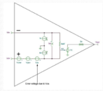
In the attached image of the non-ideal op-amp, the quantities CMRR, PSRR, and Vos are modelled as voltage sources at the nin-inverting terminal. These sources together will offset the output with some value.

If I am interesting on finding the input offset voltage, how can I know that this output shift is not a result of the other two components CMRR and PSRR ?

Thank you
opa.PNG
 

With typical or nominal supply voltage the PSRR caused offset is 0V, and in the middle of the common mode voltage range the CMRR caused offset is also 0V. The offset from mismatch should be measured with these conditions.
 
With typical or nominal supply voltage the PSRR caused offset is 0V, and in the middle of the common mode voltage range the CMRR caused offset is also 0V. The offset from mismatch should be measured with these conditions.

Dear Frank,

Thank you for your reply,

Why you think in the middle of the ICMR the CMRR cause zero output voltage ?

Secondly, I want to simulate the Vos over the entire range ICMR, what will be the explanation of this graph, or we should rather simualte CMRR over ICMR ?

Thank you
 

I don't think it is totally zero, you are right, but this is the practical way. There you can assume its effect is minor compared to mismatch.
And CMRR at DC should be negligible, if you want to know the mismatch's effect at the sides of ICMR for example for a rail2rail input amplifier you can simulate it with the condition that the CMRR is negligible. This is simple engineering not rocket science.
 
Thank you Frank,

Now I can say that offset voltage we measure or simulate is actually combination of or sum of input different errors, together they all shift the charasterics of the op-amp and one need to compensate it. The only difference between the mismatch offset and other types are the former one is frequency dependent.

I believe it is also importnat to simulate the offset voltage error for the hole range of ICMR
 

Status
Not open for further replies.

Part and Inventory Search

Welcome to EDABoard.com

Sponsor

Back
Top