Continue to Site

Welcome to EDAboard.com

Welcome to our site! EDAboard.com is an international Electronics Discussion Forum focused on EDA software, circuits, schematics, books, theory, papers, asic, pld, 8051, DSP, Network, RF, Analog Design, PCB, Service Manuals... and a whole lot more! To participate you need to register. Registration is free. Click here to register now.

how to design the layout of an nwell Resistor

Status
Not open for further replies.

Rcy

Junior Member level 1
Joined
Sep 17, 2010
Messages
16
Helped
2
Reputation
4
Reaction score
2
Trophy points
1,283
Activity points
1,389
Can anyone say me how to design the layout of an nwell resistor of value 10K. I am trying to design the resistor in magic layout tool. please help..
thanks in advance
 

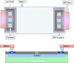
This is a simple well resistor under STI (Field), the cross section shows an NWell resistor.
For better isolation the resistor could sit in another well (for a triple well process). It could also be surrounded by an isolation ring and could have a metal field plate over the top of the resistor body.
 

Attachments

  • NWell Res.jpg
    NWell Res.jpg
    102.1 KB · Views: 353
  • Like
Reactions: Rcy

    Rcy

    Points: 2
    Helpful Answer Positive Rating
For Nwell resistor, usually it is hot Nwell (is not connecting to the highest voltage). So a P+ guard ring around it is needed.
 
Status
Not open for further replies.

Part and Inventory Search

Welcome to EDABoard.com

Sponsor

Back
Top