Continue to Site

Welcome to EDAboard.com

Welcome to our site! EDAboard.com is an international Electronics Discussion Forum focused on EDA software, circuits, schematics, books, theory, papers, asic, pld, 8051, DSP, Network, RF, Analog Design, PCB, Service Manuals... and a whole lot more! To participate you need to register. Registration is free. Click here to register now.

how to design a test jig?

Status
Not open for further replies.

syazelle

Newbie level 2
Newbie level 2
Joined
Jun 28, 2010
Messages
2
Helped
0
Reputation
0
Reaction score
0
Trophy points
1,281
Location
France
Activity points
1,308
Hello,

I got some questions regarding the test jig. If I'm well informed, a test jig is used to verify the connections between components on an IC or carry out continuity test, or testing the microcontroller or maybe resistance testing.

I woud like to know, how is it possible to design a test jig that can do all of the tests mentioned above?

I'm working on an intern project on designing a test jig for an electonic board. The problem is I don't know how to start and what should I do at the first place.

Maybe some one could give me a proper string so i can google the docs required.

Thanks.
 

Take care with the terminology, "test jig" is sometimes used to refer to a "bed-of-nails" test fixture or similar device which makes physical contact with the unit under test.

You may find the phrases In Circuit Test, Automated Test Equipment and Analogue Signature Analysis useful.
 

A test jig could be a few things.
1. A prototype tester that is designed and build by engineer or in your case intern to do fairly simple tasks such as Voltage and current tests, particular signals, resistance etc, and test for proper code on chips. If you are only testing a small portion of device or device is fairly simple you could possibly design and build your own test jig/fixture.
2. A Test fixture created by an outside source to run an entire series of tests of entire device controlled by software. This type of fixture would be used in production usually at the assembly phase to test for opens, shorts, bad solder joints, current capacity, proper timing, proper component values, etc. It will even test proper code on chips. To emplement this type of tester you will need to provide acces for probes on pcb. There are rules that need to be recognized. Such as probe to probe spacing, probe to component spacing, and weather you want this to be a top side only, or bottom side only test. Or if you will be creating a tester that has both top and bottom side probes. The later will cost alot more money. One thing I suggest is if you are going to have this type of test is to make sure and consult outside source on what there capabilities are. They will also be able to provide a lot of information on probes and probe spacing, etc...

Eda
 

thank you rob and eda for your help,

i now have clearer vision on how this things really works. In fact, my company have given me a list of test that should be done for my UUT.

1) contact test on the board
2) communication test between the µC and its peripherals
3) verifying transistor switch commutation
4) verifying memory on board
5) verifying DAC output when temperature increase
etc....

So, my test fixture should be able to run all these tests. :cry:

I've done some reading, and to do all these tests, automate software (such as Labview) is compulsary. Or do I have to develop the programs myself since the tests are for a specific board? Also, I don't think there are already existance test fixtures on the outside source that could do these various tasks. Or maybe I'm wrong.

And finally, if I'm going to do a prototype for my test fixture, this will include mechanical knowledges on fixing the test pins etc.. isn't it?

I'm sorry for blurting all of these questions. Franckly, I'm quite lost on this project. I only got two months and I'm not sure how far this project can go in this period of time.

Thanks again! I will really appreciate your help. Anyone. :)
 

That sounds a very comprehensive set of tests for one piece of test apparatus!

Normally environmental testing would not be performed on a PCB in such a test fixture.

Is this a high-volume test application? Two months is not a great deal of time. Would functional testing be sufficient?

I would consider running test code on the boards to verify most operation or using JTAG for boundary scan.

The integrity of the assembly, passive components and most active components could be assessed using Analogue Signature Analysis (check Huntron website). That would provide a flexible test solution for future use but at a cost.

Were any testability features built into the hardware such as test points?
 

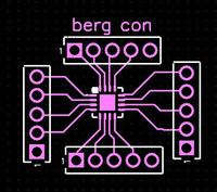
Does any know how to make a test jig that can be used to proble a QFN probe soldered on a PCB?
As the pitch of the QFN chip is about 0.6 mm pitch .. I need to figure out some way to probe some but not all pics of the QFN chip.
 

Does any know how to make a test jig that can be used to proble a QFN probe soldered on a PCB?
As the pitch of the QFN chip is about 0.6 mm pitch .. I need to figure out some way to probe some but not all pics of the QFN chip.

will such a setup do? use seperate two pin connector for DC supply and use necessary decoupling capacitors..
 

Status
Not open for further replies.

Part and Inventory Search

Welcome to EDABoard.com

Sponsor

Back
Top