Continue to Site

Welcome to EDAboard.com

Welcome to our site! EDAboard.com is an international Electronics Discussion Forum focused on EDA software, circuits, schematics, books, theory, papers, asic, pld, 8051, DSP, Network, RF, Analog Design, PCB, Service Manuals... and a whole lot more! To participate you need to register. Registration is free. Click here to register now.

How to choose right voltage reference for DACs?

Status
Not open for further replies.

fby1029

Newbie level 4
Newbie level 4
Joined
Dec 21, 2010
Messages
5
Helped
0
Reputation
0
Reaction score
0
Trophy points
1,281
Activity points
1,332
now i must design a reference for a 16-bit DAC, but i don't make a clear understanding of the requirement.

maybe the TC should be less than 1 ppm/C, but some DAC datasheets suggest 4ppm/C is also OK. i am confused about the limitation.

can someone help me?
 

HI fby 1029,

I dont think that the TC should be less than 1 ppm/c. I think you will have more problem in reduce the impact of fabrication process in the value of your reference voltage. The output noise should be a concern too.
What about the current do you need?! Do you intend to use a buffer or a low-impedance voltage reference?
I would use a low-impedance voltage reference in order to avoid a buffer. It would add a error voltage (offset voltage) that, probably, will damage your temperature performance (more than 10 ppm/C).

IF possible, tell me the link that suggest the use of reference with less than 1 ppm/C. We can discuss it.
Regards,

thanks, palmeiras

my idea comes from the ADI "Data Conversion Handbook", here's the discussion part:
https://i29.photobucket.com/albums/c252/sonofwind/edaboard/tcrequirements-1.jpg

but to offer such a reference is nearly impossible, do you think i must choose buried zener structure rather than band-gap? and the noise performance of buried zener is also better.

i have no idea about low-impedance voltage reference? do you mean a reference with bipolar class AB output stage? can you suggest me some papers or other documents about this?

is band-gap reference useless in 16 or higher bit DAC? i really fell confused.

thank you for your reply!
 

Hi fby1029,
I think that I´ve written a wrong information. I´m sorry for that. Thinking again:

1) Calculating your VLSB:
VLSB = VREF/2^N, Considering that your VREF = 1.2 and N = 16 , VLSB ~ 18 uV

2) Considering that your reference voltage can vary only VLSB/2 ~ 9uV, in a temperature range of 100 C, we have:
TC = delta VREF / delta TEMP =~ 9uV/50 = 0,18 uV/C ~0.18 ppm/C
*I have considered that delta temp = 50 when the output of bandgap references has parabolic curvature.

I am little bit surprise with such precision. As you told me, it is really hard to achieve such requirement. I have only worked with 10-bit ADCs… and traditional topologies of BGRs were enough. Anyway, I have read some papers in literature that can achieve less than 1 ppm/C (but I have never implemented them).

1) A Sub-1ppm/℃ High-Order Curvature-Compensated Bandgap Reference
(**broken link removed**)

2) 3rd order curvature corrected bandgap cell: (IEEE Xplore - Sign In)

Regarding low-impendance voltage references, take a look in this paper and it will be clear: “Low-output-impedance 0.6 lm CMOS sub-bandgap reference”
(**broken link removed**).
In few words, if you avoid an extra buffer, you will reduce this extra source of temperature error (offset voltage).

Regarding the noise behavior, do you have option to fabricated zener in your substrate? However, I thought that CMOS voltage references have better noise performance than zener diodes. Making a good design, you can reduce the low – frequency noise. About high-frequency, you can use capacitors to filter your output.

In respect of your last question: I still think that you can use BGR in such high precision applications. But this design is not simple and, probably, you will need to trim your reference.

Tell me how your work is doing, and we can discuss more about it.

Regards,
 
HI palmeiras,

Thank you very much. I will read these papers.

I think I make a mistake at the beginning. I should have cleared the specs of the DAC at first.
Now I use ADI AD5754(for example) as the target DAC. I need to design a voltage reference suited for it at least.

The AD5754 has a fair INL, +-16LSB as mentioned in the datasheet(http://www.analog.com/static/imported-files/data_sheets/AD5724_5734_5754.pdf).
If all INL contributed by reference, the TC must be under about 4 ppm/C (VREF/2^16 * 32(since +- sign) / 125(-40~+85 industrial temperature range)). Still a hard work. And the actual TC value must be better than this, of course.

But let's take a look at other 16bit DACs which have internal reference.
Maxim MAX5650 has a better INL performance(+-4LSB)(**broken link removed**) with a integrated 10 ppm/C bandgap reference.

Maybe there is some methods to adjust the DAC to small reference drift. Can it be realized? What do you think? And now I think band-gap is OK.

My design aim at integrated into DAC chip, not for external. Initial accuracy and noise performance are also important. With 5-V BiCMOS process. Do you have some recommended structures to achieve my goal? THANKS.

p.s: I may choose brokaw's cell, with chopper amp.
 

Hi fby1029,

One question: What is the value of reference voltage required by your DAC? I~m saying this because temperature coefficient (ppm/C) is a relative parameter whose value is given by
TC = (1/VREF) *(delta_VREF/delta_TEMP)

Thus for high values of VREF (4 volts, or 2 volts).... it is not difficult to achieve low values of TC. In the other side, I would like to see 1 ppm/C output reference whose value is 500 mV. Have you understood what I mean?!

But you are right…. For the Max converter, with INL = +or- 4*VLSB, the required bandgap reference is only 10 ppm/c. This shows that it is not required an exceptional temperature performance. I guess that the whole converter circuit changes with temperature, and therefore, there is no need to have the output reference so fixed.
In your case, as your INL is even worse, you will not probably find problems in achieved the required temperature coefficient. By the way, I have only one comment regarding your calculations: I would consider delta temp equal to 65 degrees rather than 125 when the output voltage has parabolic curvature over the temperature range.
Regarding your suggestion of chopper amplifier, you will solve your noise issue. Take a look in the following documents; it talks about noise in voltage references: https://focus.ti.com/lit/an/slyt331/slyt331.pdf, https://focus.ti.com/lit/an/slyt339/slyt339.pdf

If you have access to ideal data converter (for instance, described in verilog-A in your simulator) you could check the impact of the reference voltage and have a more clear view about this subject. But again, I still think that the biggest problem is the impact of fabrication. While temperature performance results in 1 mV of variation, after fabrication your reference can vary 30 – 60 mV - depending on your design. I would pay attention on this issue.

I will think a little bit more about which architecture to suggest you.

Regards,
 

HI palmeiras,

Vref=2.5V, with supply voltage about 3.3V-5.5V. I have read more papers about BiCOMS/Bipolar bandgap reference. You are right. Higher supply voltage can reduce the difficulty and simplify the question. I feel more confident that I can do the job. Thank you again.

The specs(draft):
Vref 2.5V
Initial accuracy +-0.1%
TC 5-ppm/C(typ) 10-ppm/C(max)
Noise 10uVp-p(0.1-10Hz) 500nV/root(Hz)

Any advice is helpful to me. I wonder if all characteristics can reach a better level.

p.s: To achieve a good initial accuracy, what shall I do within circult or layout level? I know trimming after fab is necessary, but I think there are other things I can do.

Best regards.
 

Hi fby1029,

--> Regarding your question about initial accuracy I believe you already know the traditional ways commonly used to reduce the impact of fabrication process:
1) Layout of bipolar and key MOSFETs in a common centroid configuration.
2) Dummy resistors and interdigitated layout.
3) Choose the type of resistor that is has the best tradeoff between (TC, matching and sheet resistance)
4) Design your amplifier to present low offset voltage. This suggestion will depend on the type of amplifier you are designing.
5) Guard rings over your reference circuit in order to isolate it from possible coupling noise of other circuits.

--> There are other techniques to improve the accuracy, but they are not so simple.
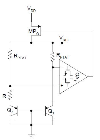
--> I would start with a traditional topology, for example given in figure 1. Because you can achieve ~10 ppm/C. Or something like: Curvature-Compensated BiCMOS Bandgap with
1-V Supply Voltage (Piero Malcovati) + a buffer, in order to reduce you temperature coefficient.

What is the current that you need to supply?

Best regards,
 
Last edited:

54_1302116630.jpg
 

HI palmeiras,

Output current is not required for the buffer belong to the input stage of the DAC.

Now I try to take packaging, devices mismatching, and resistor tolerance into account to predict potential reference voltage drifts. With all have been done, I think I can work out a reasonable specs.

Thank you veeeeery much!

Best regards,
 

Status
Not open for further replies.

Part and Inventory Search

Welcome to EDABoard.com

Sponsor

Back
Top