Continue to Site

Welcome to EDAboard.com

Welcome to our site! EDAboard.com is an international Electronics Discussion Forum focused on EDA software, circuits, schematics, books, theory, papers, asic, pld, 8051, DSP, Network, RF, Analog Design, PCB, Service Manuals... and a whole lot more! To participate you need to register. Registration is free. Click here to register now.

How export STEP model of PCB from Altium?

Status
Not open for further replies.

carpenter

Full Member level 6
Full Member level 6
Joined
Jul 25, 2012
Messages
358
Helped
22
Reputation
44
Reaction score
24
Trophy points
1,298
Activity points
4,535
I need render 3D model od PCB designed in Altium Designer , I need render qigh quality Picture.
My idea is export full PCB from Altium as STEP and this import in any CAD as Inventor or SolidWorks.
Unfortutately, if I export STEP of PCB from Altium this file contalin 3D STEP model all component, 3D Step MODEL PCB substrate and hole, but not include any track, Description layer and solder mask.

Advice on how to export include tracks and descriptions?
 

As far as I know, exporting your PCB as a step file only includes the 3D body information and PCB substrate. The other objects like tracks, silk, etc. are not included. If the additional details are required, I use a combination of the exported step file and layer specific DXFs to communicate the required info to our mechanical team.
 

Obviously you're right.
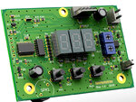
The aim is to see something like Figure.
Exported from AD and rendered in SolidWorks
Can you advise how to do it?
front.jpg
 

Unfortunately I'm not too familiar with SolidWorks' capabilities, and our engineering department hasn't had the need to produce realistic 3D models of the PCB outside of Altium. The generic step models that Altium provides are sufficient to check our mechanical clearance and the DXFs will provide information on the location of any other constraints.

However, it would be nice to produce results similar to what is shown in your attached image if possible. Is that image you provided from SolidWorks, or is it a 3D image captured from a PCB design package like Altium? The quality looks great, so perhaps it was created completely in SolidWorks or some other CAD program with potentially significant additional effort.
 

It's not a an advertising picture from Altium, it is a real design that was exported from AD, imported into Solidworks and SW was exported this file. Author's a little envelope with reflections, but otherwise good work.

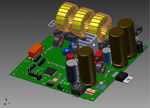
Trainer, I exported *.Step from AD and loaded it into Inventor. Here is the result.
Unfortunately, missing tracks, masks, description and I also played with setting quality rendering reflections. Pure and loaded in the base (small) resolution of the saved image.

VF.png
 

Status
Not open for further replies.

Part and Inventory Search

Welcome to EDABoard.com

Sponsor

Back
Top