Continue to Site

Welcome to EDAboard.com

Welcome to our site! EDAboard.com is an international Electronics Discussion Forum focused on EDA software, circuits, schematics, books, theory, papers, asic, pld, 8051, DSP, Network, RF, Analog Design, PCB, Service Manuals... and a whole lot more! To participate you need to register. Registration is free. Click here to register now.

How could I know the exact gain of a SC integrator?

Status
Not open for further replies.

BackerShu

Member level 3
Member level 3
Joined
Dec 22, 2007
Messages
57
Helped
1
Reputation
2
Reaction score
0
Trophy points
1,286
Location
USA
Activity points
1,795
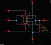
Hello, guys! I have a SC integrator shown as following.
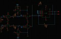
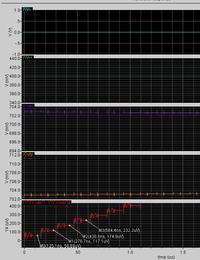
I want to fix the gain at 1/2. So I set C1 and C2 at 2.5pF, C3 and C4 at 5pF, and the gain will be C1/C3=1/2 theoretically. When I give input signal biased at 700mv of which the amplitude 500mV, and the frequency is 25KHz. The simulation result turns out to be like this.
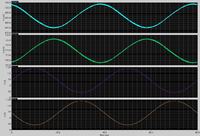
The question is I don't know whether the gain of the integrator is 1/2. And how could I know the exact gain is through the result? Please help me, thanks in advance.

Best wishes!
 

Quote:.....the gain will be C1/C3=1/2 theoretically.......

I did not look into your circuitry, however, as far as I know is the time constant of the S/C integrator and, hence, the gain at a certain frequency dependent also on the clock rate.
 

thanks LvW.

the clock frequency is 6.4MHz in this circuit. Exactly,what i mean is that C1/C3 is the integrator gain duing each clock period. Am I right?

Another question I concern is that whether the output signal reasonable because it's amplitude is so small, even smaller than the input signal. I want to use the integrator in a 2rd DT sigma-delta modulator. Will it work well?
 

hi BackerShu,

theoretically the gain of integrator is C1/C3, but the exact gain is depend on C1/C3, the dc gain and bandwidth of opamp. in general the mismatch error of capacitors is 0.1%, and the error due to dc gain of opamp is ~1/A, the error of bandwidth is C1/C3*exp(-t/tau) if no slew rate.

you can check the gain of integrator comparing output voltage to input voltage during one clock period, and (vout(n)-vout(n-1))/(vin(n)-vin(n-1)) is equal to gain.
 

If the output is smaller than the input signal, that means you are working with a frequency well above the crossover frequency (0 dB).

Nevertheless, ´bBecause the circuit diagram is rather involved, it would be helpful to see a simplified diagram with switches, capacitors and opamps only.
 

Thanks!

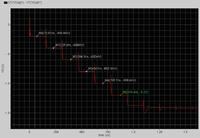
To jiangxb: what is tau? Could you explain it to me please! As to measure the gain, I set the input signal a 400mv dc signal. Does it mean that Vout(nT)-Vout((n-1)T) equals 200mv every clock period? But I got the following result.

It seems the Vout only increased by 50uV every clock period. What the problem in my circuit will be? And the overshoot is so big, does it mean the opamp's phase margin is not enough?

To LvW:the input signal frequency is only 25KHz, and the opamp's GBW is about 100MHz. It can't be above the crossover frequency,I think. There are nothing more than switches, capacitors and opamps in my diagram. The TG symbol is only a CMOS switch.

Best wishs!
 

hi BackerShu,

tau is bandwidth of integrator tau=f*gbw, there f is feedback factor and gbw is unity gain bandwidth of opamp. i notice that there is a lack of switches which should connect v1+ and v1- to vcm, otherwise the charge of sampling capacitor can't transfer to integration capacitor.
 

    BackerShu

    Points: 2
    Helpful Answer Positive Rating
Quote: tau is bandwidth of integrator tau=f*gbw, there f is feedback factor and gbw is unity gain bandwidth of opamp

This can´t be true. The unit of tau is "time" and the right side of your equation is a frequency. According to the conventional nomenclature, tau is the integration constant of the integrator. In the BODE diagram, the magnitude function of the integrator crosses the 0 dB-line at ω=1/tau.

To BackerShu: This value of ω is called "cross-over frequency". And this has absolutely nothing to do with the GBW of the opamp.

Added after 6 minutes:

BacherShu: I am rather lazy, and it is not too easy for me to verify the function of the switches (that means: to separate and verify the two phases of the switches which is very important).
Therfore i have asked you to provide a simplified block diagram. So it would be much more easier to answer your question.
 

    BackerShu

    Points: 2
    Helpful Answer Positive Rating
Hi jingxb.

Thank you very much for your explaining!
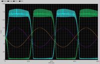
You're totally right. I've added the switches, and got the reasonable result as shown in Fig 1 with a input signal -- 400mv dc .

Another question is that ,as you can see, there're many sentus in the output signals.

Will they influence other circuits greatly? If so. What method canbe used to weaken or avoid the sentus. Maybe you have already known that I want to use the integrator in a DT sigma delta modulator.

Regards!

Added after 34 minutes:

Hi LvW!

So w is the time constant of the intagrator, and is related to the Req and Ceq of the opamp input node. W equals to 1/Req*Ceq cursorily. Am I right?

I'm sorry to misunderstand what you mean. In fact, I've no idea about separate and verify the two phases of the switches. I just set Clk and Clkb (the two have 180degrees phase differance)to drive the two mosfets. The switch is shown in Fig 1. Is there anything wrong with it?


Another question:The modulator I want to implement is shown in Fig 2. It makes me some difficult to design the feedback circuits. The circuits that return the result of the comparator and control the Vref+ and Vref-Could you give me some useful reference?Thank you!


Regards?
 

hi LvW,

my fault, the right equation is tau=1/(f*gbw) which is the time constant of integrator during integration phase. considering bandwidth only the output of integrator is vout(n)=vout(n-1)+C1/C3*vin(n-1)*(1-exp(-t/tau)).

hi BackerShu,

these two phase clocks are non-overlapped as two-phase clock scheme in figure and S1 and S2 are ayed-version of S3 and S4 for bottom-plane sampling. clk and clkb are right in your fig. 1, but in general the width of pmos in TG is 2~3 times larger than nmos for better linearity. the glitch is normal.
 

Hi BackerShu,

something is not clear yet.
Quote:
So w is the time constant of the intagrator, and is related to the Req and Ceq of the opamp input node. W equals to 1/Req*Ceq cursorily. Am I right?

Not w but instead 1/w equals the time constant.
Think of a simple time continuous Miller integrator which has a time constant of tau=R1*C2. By replacing this circuit with its S/C equivalent the time constant becomes tau=Ts*C2/C1 with Ts=sampling intervall and switched C1 replacing R1.

Now I have recognized your switch arrangement. Its a simple CMOS switch with on/off function. My question was because it could be something like a toggle switch which is used for bilinear resistor replacement.

Hi, jiangxb
Quote: my fault, the right equation is tau=1/(f*gbw) which is the time constant of integrator during integration phas

I cannot see how the gbw of the opamp should determine the time constant of the integrator; can you explain this ? For my opinion, the correct definition is given in my comment above.
 

hi LvW,

now i understand what you mean. the time constant i mentioned is within one phase, i.e. integration phase or charge transfer phase. what you mean is looking at the integrator during a long period, and it's right from this.
 

OK, I see. Your time constant belongs to the charging process of the capacitor.

But, nevertheless, there is no influence from the gbw of the opamp.
The charging constant is primarily determined by Rswitch*C, with Rswitch being the switch resistance itself.
 

hi LvW,

the resistance of switch and capacitor influence the settling of output voltage of integrator indeed, but the dominating reson is bandwidth of opamp and feedback of integrator during charge transfer phase. when the charge on sampling capacitor transferring onto integration capacitor the speed of opamp dominates the settling speed of output voltage of integrator. you can refer to Piero Malcovati's "Behavioral Modeling of Switched-Capacitor Sigma-Delta Modulators".
 

Status
Not open for further replies.

Part and Inventory Search

Welcome to EDABoard.com

Sponsor

Back
Top