d123
Advanced Member level 5

Hi,
Sorry, this thread/question will be hard to understand from the assorted hand-drawn schematics and my usual endless blather, even for me, so not expecting much inclination for anyone to parse the images of sub-circuits and the lengthy descriptions. Anyway, any help appreciated.
Circuit design goal was a 'non-retriggerable, once and once only one-shot with negative-going input signal'. Achieved, except did positive-going input. It reeks of hobbyist territory but is quite flexible as a circuit...
Description by stages:
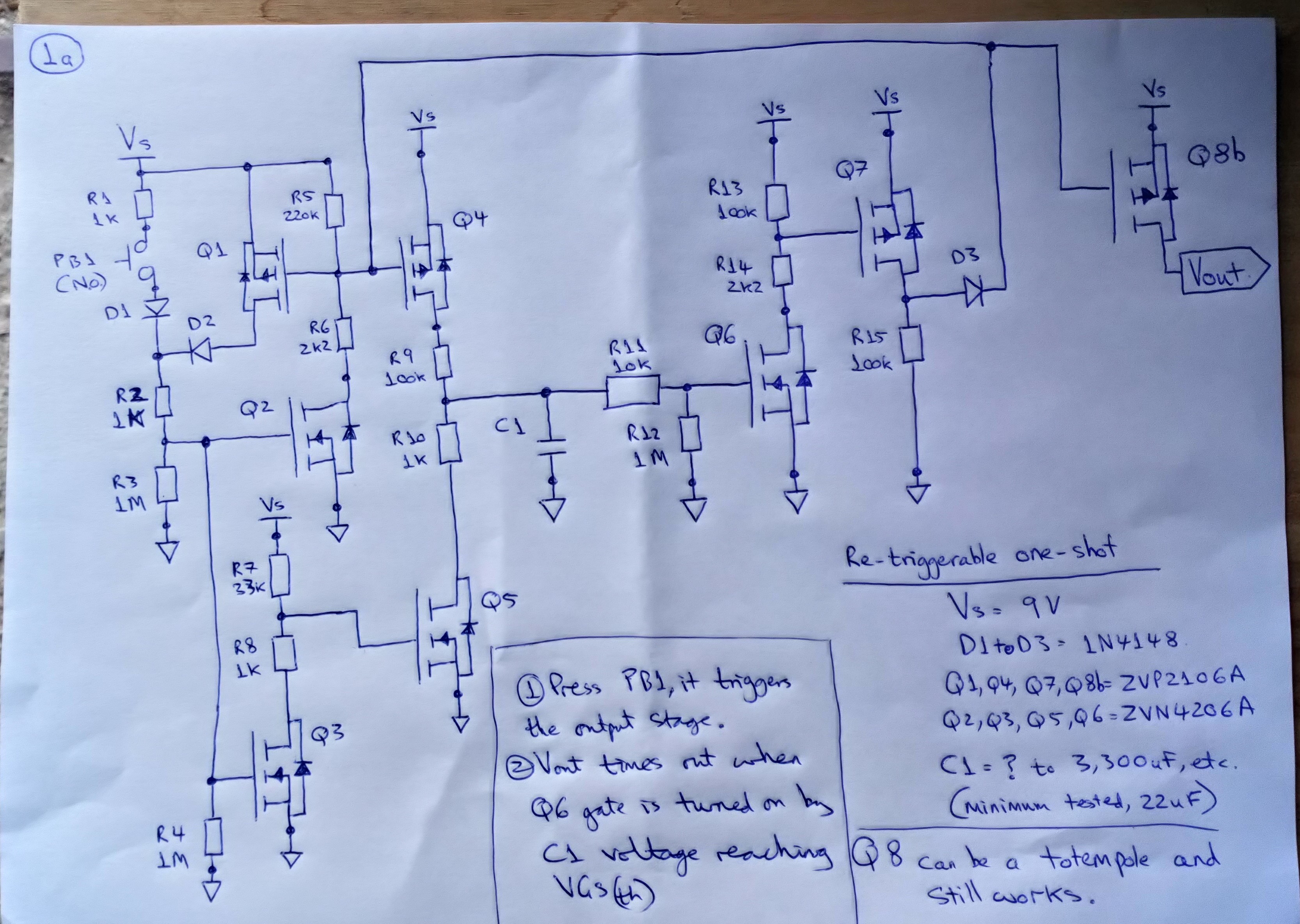
A re-triggerable monostable:

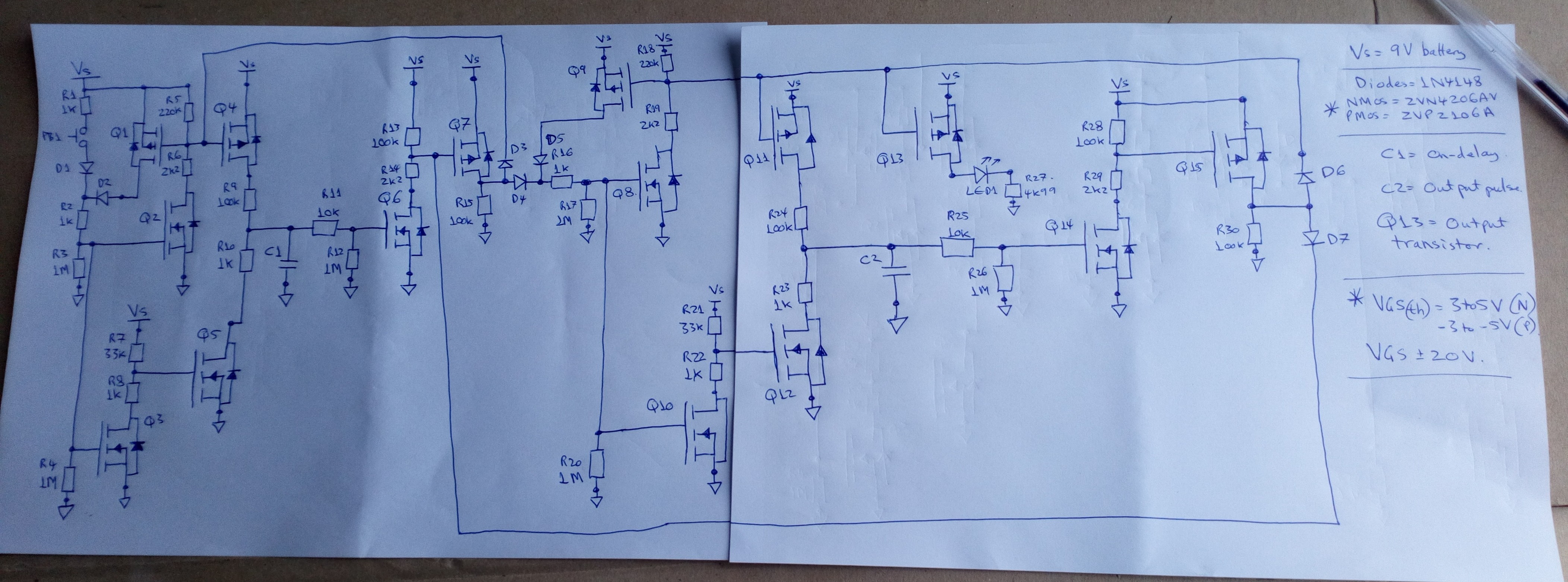
A re-triggerable monostable with on-delay:

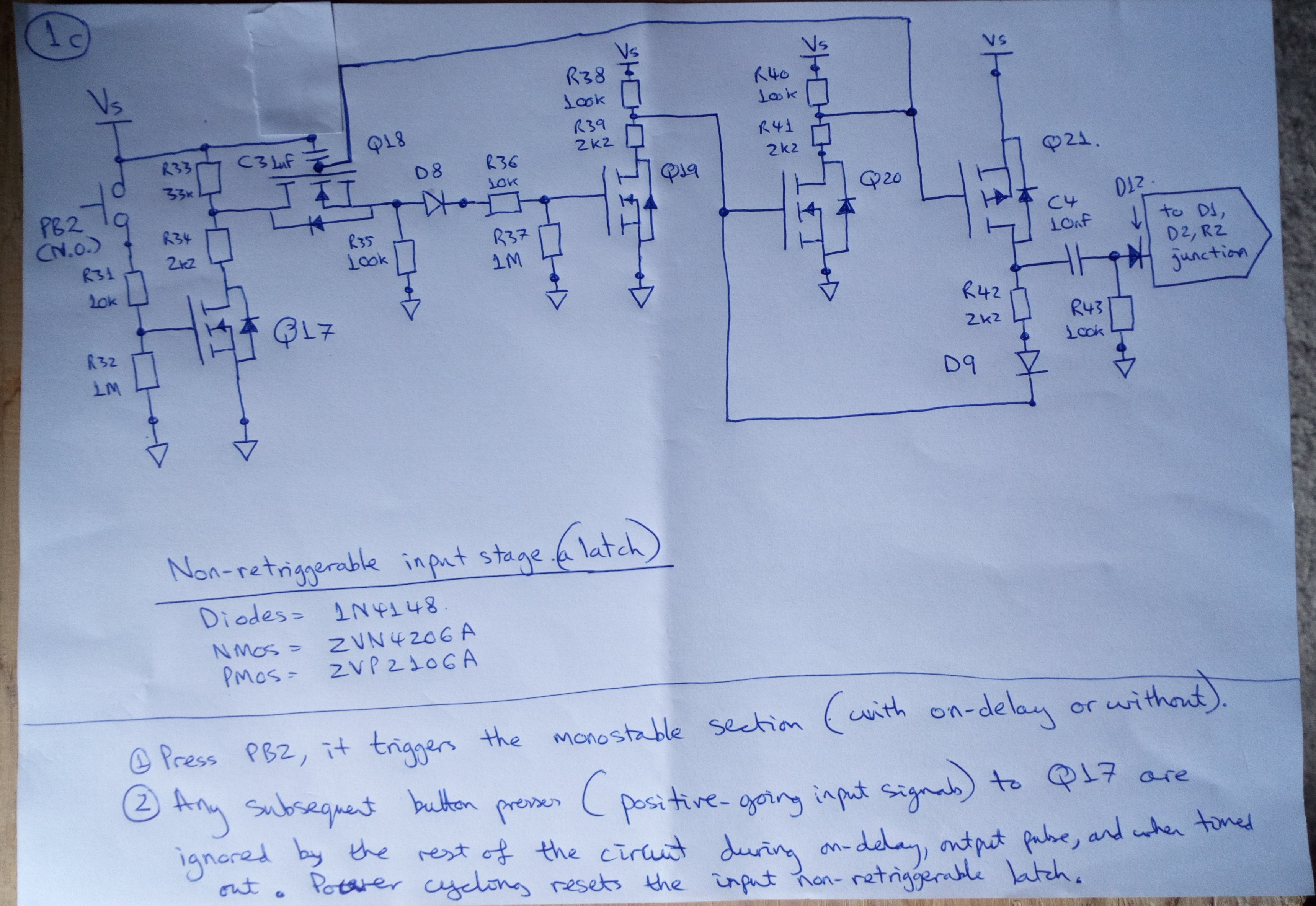
Adding this section makes it a non-retriggerable, once and once only monostable that power cycling resets:

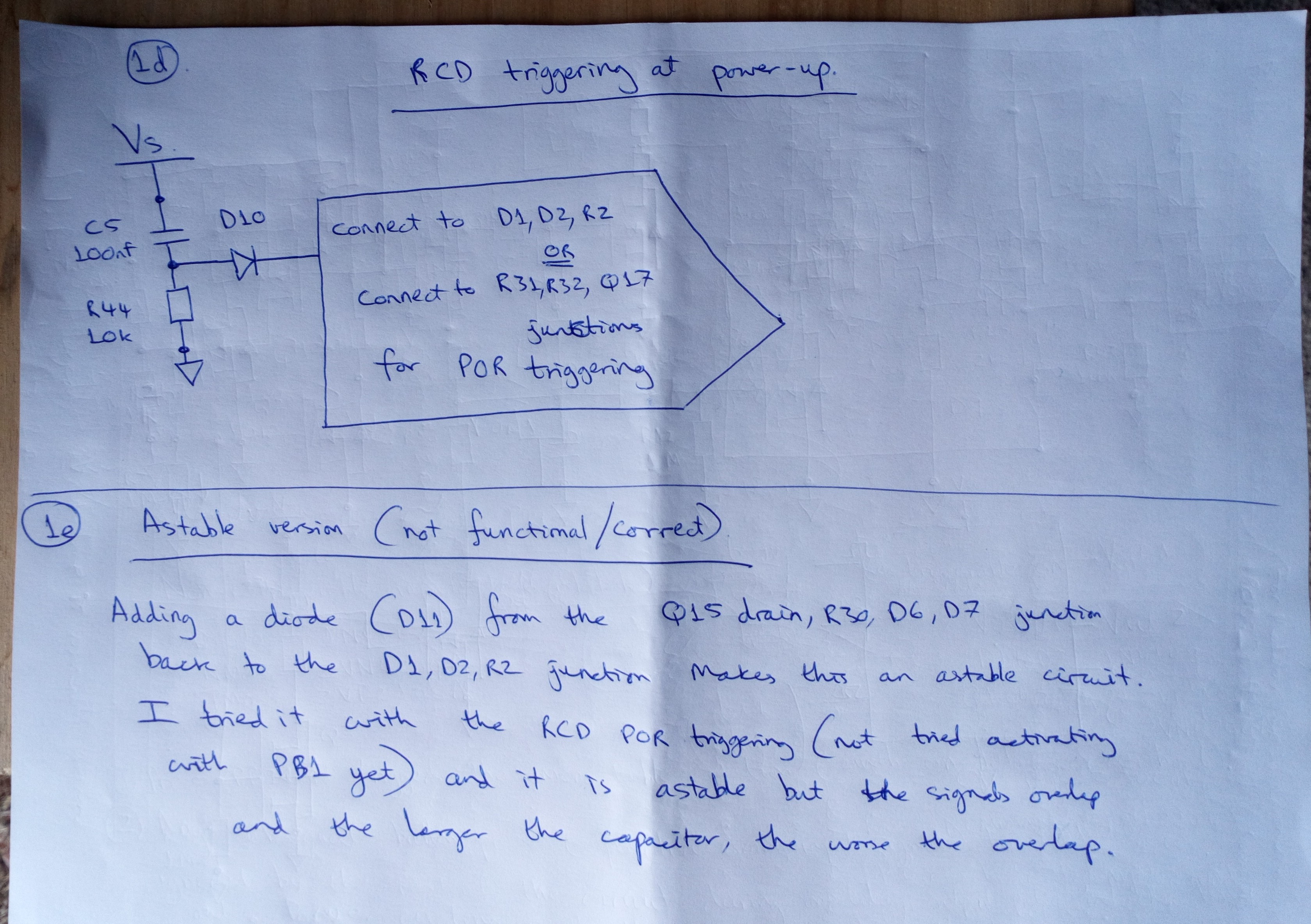
It only needs a POR RCD to auto-trigger at power-up:

... I got 'mission creep' syndrome and out of my admiration for Hans Camenzind and his incredibly versatile and ubiquitous (but we all criticize it...) clever little timer IC, I wanted to get my circuit to at least do astable as well - mark-to-space is set by C1 and C2 selection in my circuit and Q13 is Vout for that (it also works with a push-pull/totempole output stage, not just a PMOS drain output).
Problem: Re-triggerable and non-retriggerable monostable with or without on-delay works great.
Astable version doesn't work - Q8b and Q13 signals end up overlapping as Q13 (C2 presumably doesn't drain as fast as needed) lingers on longer than desired and so Q8b turns back on too soon. The larger the capacitors, the worse it becomes, until it's embarrassing to look at.
I tried making R10 and R23 100 Ohms to drain the timing caps faster but it makes no difference. I made some of the 2k2 sink resistors 330 Ohms to speed up turn off, but it makes no difference. Will try changing R11 and R25 1k in case that helps.
Any suggestions or guesses as to why the astable signals end up overlapping, even if C1 is only 100uF and C2 is 220uF?
Thanks.
Sorry, this thread/question will be hard to understand from the assorted hand-drawn schematics and my usual endless blather, even for me, so not expecting much inclination for anyone to parse the images of sub-circuits and the lengthy descriptions. Anyway, any help appreciated.
Circuit design goal was a 'non-retriggerable, once and once only one-shot with negative-going input signal'. Achieved, except did positive-going input. It reeks of hobbyist territory but is quite flexible as a circuit...
Description by stages:
A re-triggerable monostable:
A re-triggerable monostable with on-delay:
Adding this section makes it a non-retriggerable, once and once only monostable that power cycling resets:
It only needs a POR RCD to auto-trigger at power-up:
... I got 'mission creep' syndrome and out of my admiration for Hans Camenzind and his incredibly versatile and ubiquitous (but we all criticize it...) clever little timer IC, I wanted to get my circuit to at least do astable as well - mark-to-space is set by C1 and C2 selection in my circuit and Q13 is Vout for that (it also works with a push-pull/totempole output stage, not just a PMOS drain output).
Problem: Re-triggerable and non-retriggerable monostable with or without on-delay works great.
Astable version doesn't work - Q8b and Q13 signals end up overlapping as Q13 (C2 presumably doesn't drain as fast as needed) lingers on longer than desired and so Q8b turns back on too soon. The larger the capacitors, the worse it becomes, until it's embarrassing to look at.
I tried making R10 and R23 100 Ohms to drain the timing caps faster but it makes no difference. I made some of the 2k2 sink resistors 330 Ohms to speed up turn off, but it makes no difference. Will try changing R11 and R25 1k in case that helps.
Any suggestions or guesses as to why the astable signals end up overlapping, even if C1 is only 100uF and C2 is 220uF?
Thanks.
