Continue to Site

Welcome to EDAboard.com

Welcome to our site! EDAboard.com is an international Electronics Discussion Forum focused on EDA software, circuits, schematics, books, theory, papers, asic, pld, 8051, DSP, Network, RF, Analog Design, PCB, Service Manuals... and a whole lot more! To participate you need to register. Registration is free. Click here to register now.

High voltage High Ron SiC mosfet. Is this simulated Ron plausible?

GLR

Newbie level 4
Newbie level 4
Joined
Jul 10, 2024
Messages
7
Helped
0
Reputation
0
Reaction score
0
Trophy points
1
Activity points
42
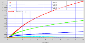
Hi guys... is it realistic the following simulates Rdson(iD) for a High Voltage SiC mosfet belonging to high-Ron class?
Is acceptable for you a similar Rdson(iD) of a commercial SiC mosfet?

What is your opinion? :)

[Ohm] vs [A]

received_26290998193847633.png
 
Last edited:
I don't recognize what you are trying to do but suspect that the left side may be channel, normal while right side is the body diode turning on at Vd<Vs? But why the non-monotonicity, no idea; have yet to look close at differences from Si power MOSFETs.
 
Thank you very much Dick... interesting your reply, but Vd is always superior of Vs (neutral).
I'm trying to design a 2000V 1000mOhm SiC MOSFET for non-linear uses
 
Current is negative and positive, Ron is always positive so voltage must be same sign as current (i.e. when current is negative so is voltage).

Maybe your test bench is not doing what you think. Try plotting the terminal voltages all at once and see if it's sensible / as-expected?
 
No, no... current is in exponential scale, is not negative. I used exponential scale on horizontal axis to "enlarge" the visual of the trend
 
Surely the logarithmic horizontal iD axis complicate the graph, perhaps unusefully...
Here the lin-lin graph

received_1674521763319479.png
 
Y axis is still Ron?

To judge MOSFET "normalness" I like plain lin-lin ID-VD,
lin-lin sqrt(ID)-VG, log-lin ID-VG.

Now how SiC MOSFET may differ from silicon in these
display-frames I couldn't say.

But normal for a MOSFET (IME) is that RON is lowest at
low Vds / lower ID and should go high / infinite once in
saturation (but SiC MOSFETs have high VT and no
telling from present info, whether Vgs is high or low
and the set of I-Vs would draw that out.

One thing that will cause the kind of "high where it
should be low" behavior of Ron, is a spacer / LDD
problem at the source side, where at low drain bias the
channel fails to "hook up" to the ohmic source (this is
a "failure of self-alignment" often by hard mask (spacer)
control (too fat, or angled implant lacks reach). Then
you can see (even in plain MOS) that Ron is high at
low Vds (like below 50-100mV) and then "snaps in"
above that point. This can be missed by characterization
if you step from 0 to "above pain threshold" in the family
of curves.

Start with the classics and you'll speak more to old timey
transistor monkeys.
 
  • Like
Reactions: GLR

    GLR

    Points: 2
    Exaustive!
Dick, your explanation is really exaustive (y).
Surely all you say is enlightening, thanks... for me to see this lin lin Ron-iD graph is more reassuring, on the other hand is only at very little iD that gives some doubts with very high Ron, then above 1A the trend is almost expected, even if Ron decreasing and then lightly decreasing. I think that above a certain iD it will start to increase.
In the simulation are inserted three non-ideality: gateox +charge, some literature interface-defects and attenuated anisotropic mobility
 
Try a very fine sweep step on the drain and keep going finer. Anything where zero meets zero is to be suspected. Your Ron as VDS/Id must fail at 0/0. If the next step is sane then maybe it's just numerical.
 
  • Like
Reactions: GLR

    GLR

    Points: 0
    Thank you so much
Is such a set of output characteristics -that has a dynamic range contained in 1V- coherent and useful in non-linear applicative uses for a 2000V - 800mOhm SiC mosfet?
 

Attachments

  • outputs.png
    outputs.png
    57 KB · Views: 38
Looks like the source-channel "hookup" has a bit of excess Ron at low Vds. This may be acceptable when you are targeting 2kV. But it might (on a real device) indicate a lithography marginality ( like what if source implant is offset more, does "hookup" fail altogether?).

In a TCAD simulation, don't know how the ohmic (you wish) or evolved source-channel connection (S-B and inversion-layer-B depletion regions meet but this needs lateral field if not complete @ Vgs=0) is expressed or solved-for. But it looks like a familiar device architecture issue in development, around the N+, NLDD, spacer feature-group.
Or what's similar in your mesh-up.
 

LaTeX Commands Quick-Menu:

Part and Inventory Search

Welcome to EDABoard.com

Sponsor

Back
Top