berger.h
Full Member level 1

High side switch - minimalize power disipation.
Hello ,
I need relise high side swith who switch 25V on load about 20 Ohm, if voltage on tracked line exceeds 4V, voltage on this line is 0-40V.
Switch transistor mus have max size SOT-223
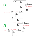
It was originally used low saturation PNP transistor any as picture A.
Power lost over Base NPN 4V 4*0,4mA=1,6mW, 40*4,8mA=192mW for 40V
Power lost over colector NPN 25V (10,7+1,23)*25=298mW
Power lost over colector PNP (25-24,91)*1,246=112mW
Overal max power lost 112+298+192=602mW
If use P-MOSFET NVF2955, picture B
Power lost over Base NPN 4V 4*0,595mA=2,4mW, 40*3,93mA=158mW for 40V
Power lost over colector NPN 25V 0,55*25=14mW
Power lost over colector MOSFET (25-24,8)*1,241=240mW
Overal max power lost 240+14+158=413mW
MOFET solution have 50% lower power lost
Qouestion
Count I correctly?
is it s an efficient solution?
has one or the other solution significantly disadvantages or risks? For example, losses in the transition state.


