Continue to Site

Welcome to EDAboard.com

Welcome to our site! EDAboard.com is an international Electronics Discussion Forum focused on EDA software, circuits, schematics, books, theory, papers, asic, pld, 8051, DSP, Network, RF, Analog Design, PCB, Service Manuals... and a whole lot more! To participate you need to register. Registration is free. Click here to register now.

[SOLVED] High insertion loss in Bandpass filter

Status
Not open for further replies.

noori.re

Member level 1
Member level 1
Joined
Sep 19, 2011
Messages
38
Helped
1
Reputation
2
Reaction score
0
Trophy points
1,286
Location
Dresden, Germany
Activity points
1,592
Hello everyone,

I have a high noise level in the rf input of PA, also there are spurs. I designed an elliptical BPF for PA input. the simulation shows everything is going to be well. but after applying it to my circuit, I see around 20 dB insertion loss in the pass band! Do you know where does it come from?

BR,
Reza
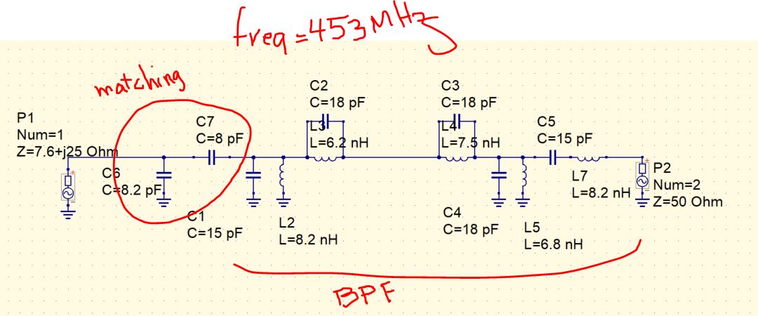
Capture.JPG
 
Last edited:

How did you implement this filter ? Which components did you use ?? How did you draw its layout ? And how did you attribute 7.6+j*25 Ohm with VNA ??
 

The PCB was designed before (6 layers). all traces are considered to be 50 ohms. I used 0201 L/C elements to implement the filter. As I didn't provision BPF before design, I had to scratch the board and make some rooms for L/C elements.
For measuring input impedance, I used somehow a precise tested method. I calibrated the VNA exactly in the location of matching NW on board using, soldering a semi-flex coax pigtail on board and connecting to VNA. The simulation result for the filter is like below but in practice, it acts like a 15 dB attenuator! In my opinion, there is something basic wrong, but I can not find it. also when I'm changing the frequency of the input signal, the final output of PA remains constant (8 dBm). it acts as a flat pass band! does it mean that this is the stop band and not the pass band?
Capture.JPG
 

Why did you design with this high Q/ small pass band. You easily get largedeviations with a few tolerances or parasitic PCB elements.
 

I couldn't get the right answers to my questions..
How did you realize filter's layout ?
Which series of components did you use ? Which brand and which series ?
How could you arrange that weird complex impedance on VNA ? Didn't you use it before or after the matching circuit ?
Has the filter 50/50 Ohm Input and Output Impedance ?
Sketch something and let us understand.
 

Why did you design with this high Q/ small pass band. You easily get largedeviations with a few tolerances or parasitic PCB elements.
Exactly. After applying the same filter on another board and measuring using VNA, I found that the tolerance of L/C elements are very high for this Q.
Is there any alternative?
--- Updated ---

did you try your simulation with tolerances? my guess is that the caps and inductors are 10%
This one is what I had to do before applying.
 
Last edited:

Tolerances shift the Center Frequency left or right or sideband suppressions are impacted. But -20 dB Insertion Loss ought to have another reason or reasons.
 
Tolerances shift the Center Frequency left or right or sideband suppressions are impacted. But -20 dB Insertion Loss ought to have another reason or reasons.
I applied the filter on another board and measured the S21. It was strangely acting like a band-stop filter! (for now, I dont have access the data to upload). My first idea is that the tolerance caused that because when I've changed the values for a wider pass band and widened the distance between nulls, it acts correctly. It seems the values should be selected in a way that the distance between nulls and peaks is not affected by the tolerance of L/C elements.
 

I have examined your filter and my conclusion is that the filter is very sensitive to tolerances and definitely to layout topology. You have to change the type of filter and try to build it up with microstrip distributed type.
Using such filter topology/configuration needs very tight and temperature stable components that is practically impossible. Therefore, you should find another filter configuration which will be less sensitive to all undesired effects.

If this filter would be a serious manufacturing, I strongly recommend you to do Monet Carlo Analysis and Pareto Analysis in order to find the Sensitivity and its Dependency. This is very important for a serious design.
 

I have a high noise level in the rf input of PA, also there are spurs
I would suggest trying to find the root cause of the noise and spurs and fixing the problem there. I expect that this will will be an easier solution to to your problem in the long run. The filtering at the PA should be for removing harmonics and may be widely spaced spurs. As BigBoss says you will need to do a sensitivity analysis, and don't forget to include variations in the load impedance, it can have a significant effect on a narrow band circuit like this. A narrowband filter like this will almost certainly need to be tuned individually.
 
In addition to the advice above: you really need to include component loss (Q factors) in simulation.

The price that you pay for small filter bandwidth is higher loss, but you don't see that if you use ideal L C in simulation.
 
In addition to Volker's comment you also need to include the PCB pads and interconnecting tracks, (preferably using an EM simulator) at 450MHz it makes a noticeable difference
 
I have examined your filter and my conclusion is that the filter is very sensitive to tolerances and definitely to layout topology. You have to change the type of filter and try to build it up with microstrip distributed type.
Using such filter topology/configuration needs very tight and temperature stable components that is practically impossible. Therefore, you should find another filter configuration which will be less sensitive to all undesired effects.

If this filter would be a serious manufacturing, I strongly recommend you to do Monet Carlo Analysis and Pareto Analysis in order to find the Sensitivity and its Dependency. This is very important for a serious design.
Thank you for your recommendations that are too much useful.
Using Microstrip line filters; I haven't tried that but because of the limitation of space that I have in the board I think it won't be applicable for me.
--- Updated ---

I would suggest trying to find the root cause of the noise and spurs and fixing the problem there. I expect that this will will be an easier solution to to your problem in the long run. The filtering at the PA should be for removing harmonics and may be widely spaced spurs. As BigBoss says you will need to do a sensitivity analysis, and don't forget to include variations in the load impedance, it can have a significant effect on a narrow band circuit like this. A narrowband filter like this will almost certainly need to be tuned individually.
Actually, The noise levle& spurs were worse than they are now, I did a lot of modifications and improved it by 8 dB! but not enough. I may open another thread for that. thank you.
--- Updated ---

In addition to Volker's comment you also need to include the PCB pads and interconnecting tracks, (preferably using an EM simulator) at 450MHz it makes a noticeable difference
You're right, with which software can it be done? HFSS? Maxwell? Does Altium have such a tool?
 
Last edited:

Status
Not open for further replies.

Part and Inventory Search

Welcome to EDABoard.com

Sponsor

Back
Top