Continue to Site

Welcome to EDAboard.com

Welcome to our site! EDAboard.com is an international Electronics Discussion Forum focused on EDA software, circuits, schematics, books, theory, papers, asic, pld, 8051, DSP, Network, RF, Analog Design, PCB, Service Manuals... and a whole lot more! To participate you need to register. Registration is free. Click here to register now.

High common mode voltage Current measurement

Status
Not open for further replies.

Amr Wael

Member level 5
Member level 5
Joined
Jul 13, 2020
Messages
84
Helped
0
Reputation
0
Reaction score
1
Trophy points
8
Activity points
866
Hello ,
I want to design a current measurement circuit using a shunt resistor that's capable of measuring up to 20Amps and can tolerate over 220 V common mode voltage.
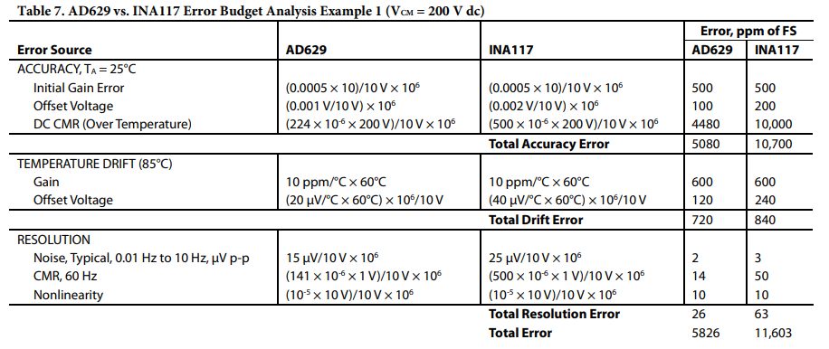
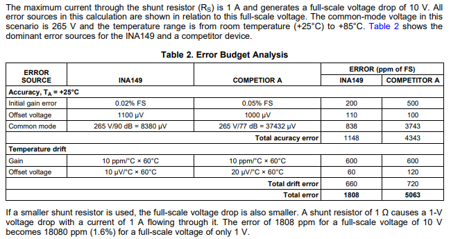
I decided to use a high side topology in which the shunt resistor is connected between the supply and the Load. i Narrowed down my choices to TI (INA149) and Analog devices (AD629). Those are high common mode voltage differential amplifiers that are capable of measuring the voltage difference on the shunt resistance. My problem is that I would like to use a resistor with a range of 10m Ohms or 5 mOhms to minimize the power disspiation but at the same time I found error budget analysis at the Datasheets of both ICs that show that the error is around 1.6% at a full scale voltage of 1V when using a resistor of 1 ohm which obv. carries a current of 1 A.
Based on the analysis I concluded that the error will be further more higher in case I decrease the shunt resistance value.
My question is How can I use such an ultra small Shunt resistance without losing accuracy?
Thank you very much in advance.
Capture1.PNG
Capture2.PNG
 

A low ohmic shunt is only feasible with a sense amplifier residing at the HV node. Respectively you need an isolated or floating power supply circuit.
 

Hi,

Depending on what you want to achieve..
ADC on the high side with isolating digital interface may be a high quality option.

We definitely need more information.

Klaus
 

I found this application note by Texas instruments , it says that a normal current sense amplifier could be adjusted using few external components to tolerate high common mode voltages
I think the circuit in figure 2is what I am looking for but I do not understand the modification that converted 60V VCMmax to 400V
--- Updated ---

i specifically don't understand this sentence in the application note
"P-channel MOSFET, Q1, as shown to cascode the output current of IC1 down to or below ground level"
 
Last edited:

A current source is used to span the voltage difference between high side and ground. Due to the low quiescent current, INA168 is well suited for floating supply. If its DC accuracy and speed is sufficient for your application, it can be low effort solution.
 

To read a sense resistor at high side, it's useful to measure relative to supply+.
This illustrates how to orient a P device, operated in common base mode.
Its power supply is a few volts. The 220V supply serves as common.

Notice it's feasible to use a .005 Ohm sense resistor. It develops 1/10 V at 22 Amperes. The transistor applies gain of several hundred, resulting in a few volts reading across the collector and base resistor.

This technique may not necessarily meet your specs for accuracy or linear performance. It requires effort to adjust values so you get zero output from zero input. Temperature variations may alter transistor response. It does have an ability to coexist with neighboring high voltage.

measure 22A high side PNP 220 VDC load.png
 

@FvM Thats exactly what I don't understand , How is the IC working if it's supply is floating? is the output transistor only what's working? I also don't understand how does a current source span the voltage difference do you mean it acts as a voltage divider in order not for the high voltage to be fully applied on the IC? I don't get the circuit if you could elaborate more i Would be very thankful
Also wouldn't this current source change the value of the output current which should be solely dependant on the opamp's output voltage (input to the output npn amplifier)?
 

Hi.

I hope I did understand your worries right...

It's like a bird sitting on a 100,000 Volts wire. It's not the 100,000V with respect to earth that counts,
There's just a tiny volts between it's feet...nothing harmful.

The same is with the IC. Not high voltage "between" he pins....only the current source transistor.

Every current measurement IC manufacturer gives information about how they work. Either in datasheets or additional documents.
I recommend to read through some of them.

Klaus
 

Capture5.PNG

--- Updated ---

@FvM Actually I understand the difference between the voltage applied on the IC and the high side voltage. My problem is related to how is this voltage divided? Why under this configuration , large voltage will develop on the PMOS current source and small voltage drop on the IC?
 

Please correct Q1 polarity, drain is connected to RL. IC and Q1 base/source voltage is defined by DZ1, drain-source voltage mainly by 400V supply voltage.
 

Status
Not open for further replies.

Part and Inventory Search

Welcome to EDABoard.com

Sponsor

Back
Top