Help Required:FOlded cascode Design

Status
Not open for further replies.

bilal_e78

Newbie level 3
Joined
Oct 4, 2007
Messages
4
Helped
0
Reputation
0
Reaction score
0
Trophy points
1,281
Activity points
1,316
Hi,

I am a very new this analog designing and i am also trying to design the same topology..

I have some problems regarding

1)hOW would i know about , that i have a correct DC operating point. I means what value of the output voltage i should expect if I used Vin+=400mV, Vin=-400mV, what should the Vout+ and Vout- should be
if Dc gain is about 30 dB.

2) I have completly studied your whole post and I m following Structure Analog CMos Design and Razavi's book for sizing of the transistors, but i m getting differnt currents and gm values from calculations.

3) Biasing of the structures, we need some voltages can any one guide what should be the good guessng way,....for starting or should I need a proper biasing circuitry and sam efor the CMFB ciruit.

Vdd = 1.2 V, Vss =0. and my GBW and SR are both very high.

Thanking in advance.


Regards
Bilal
 

Regarding you First Question

gain = 30 db which is about 31.66 assuming its 20log(vout/vin)

and you input differential voltage is Vin+ - Vin- which is about (400mV - (-400mv) = 800mV) ..
with that high gain as per equation you should get close to 25.44 V.
Your, Vdd - Vss is about 1.2v so your output cannot go beyond 1.2V ideally , cosidering some minimum voltage drop accross the cascode transistors it cannot go beyond 1v .... so you will get a saturated output ..

For the other questions you might want to post a schemtic diagram for a better response.. But in general keep the Vin -Vth for the amplifier transistors close to 100mv considering that your Vdd-Vss is quite low...

Added after 1 minutes:

Regarding you First Question

gain = 30 db which is about 31.66 assuming its 20log(vout/vin)

and you input differential voltage is Vin+ - Vin- which is about (400mV - (-400mv) = 800mV) ..
with that high gain as per equation you should get close to 25.44 V.
Your, Vdd - Vss is about 1.2v so your output cannot go beyond 1.2V ideally , cosidering some minimum voltage drop accross the cascode transistors it cannot go beyond 1v .... so you will get a saturated output ..

Generally the input voltage levels for cascode amplifiers is very low iun the range of a few millivolts

For the other questions you might want to post a schemtic diagram for a better response.. But in general keep the Vin -Vth for the amplifier transistors close to 100mv considering that your Vdd-Vss is quite low...
 

    bilal_e78

    Points: 2
    Helpful Answer Positive Rating
Hi,

Thanks for you responce, to u it might sound a bit stupid as i m a newbie, i cant undrstand as my gain is like 31.66 but my DC output as u mentioned never crosses the 1.2 ,
also all my caclulated values of currents differ from simulated ,,,, how can i be sure about that my DC operating is good
2)
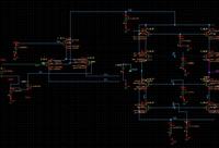
I am attachin my shcematic , plz have a look and identify any faults.......
and when i do ac anlaysis my output never crosses the 200mv limits.

Thanks for ur responce also do comment abt the biasing .....and also ant cmfb


REgards
 

Plz reply............................. I really need help regarding this

Best Regards
 

Check to make sure every one of your transistors is biased in forward linear mode. For bipolars this means Vbe>0 and Vbc<0 for NPN and for mosfets this means vgs>0 and vds>vgs for NMOS. Reverse for P devices. SPICE will pop these values out for all transistors in the raw simulation output. It should be your first sanity check if your simulation doesn't look right (and even if it does - simulators can fool you).
 

Status
Not open for further replies.
Cookies are required to use this site. You must accept them to continue using the site. Learn more…