Continue to Site

Welcome to EDAboard.com

Welcome to our site! EDAboard.com is an international Electronics Discussion Forum focused on EDA software, circuits, schematics, books, theory, papers, asic, pld, 8051, DSP, Network, RF, Analog Design, PCB, Service Manuals... and a whole lot more! To participate you need to register. Registration is free. Click here to register now.

HELP!! Can help me check my dc chopper circuit?

Status
Not open for further replies.

CandleCookie

Advanced Member level 4
Full Member level 1
Joined
Aug 25, 2010
Messages
102
Helped
11
Reputation
22
Reaction score
11
Trophy points
1,298
Location
Malaysia
Activity points
2,069
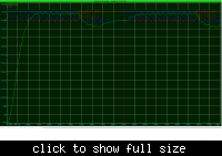
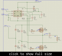
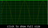
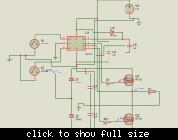
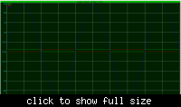
My circuit didn't work well. I don't know what is the problem. When the Vgs2 is on, the current should be in the negative side and go back to zero when both switches are off.
 

Attachments

  • Untitled1.png
    Untitled1.png
    24.4 KB · Views: 191
  • Untitled2.png
    Untitled2.png
    32.2 KB · Views: 152

Try to simulate with pulse controlling Q1 is the negation of pulse controlling Q2. If both Q1 and Q2 is on at the same time, it will short the Voltage source.
 
When the Vgs2 is on, the current should be in the negative side
You mean negative current polarity? To get a negative current with a resistor load, the output voltage must be negative, too. That's not possible with this circuit. There are however various issues:

- The gate voltage for the highside switch Q1 must be applied between gate and source, not between gate and circuit ground. Now Q1 doesn't turn on completely, as a result, the output voltage (and current) is only a small fraction of the value in regular operation.
- IRF250 has a gate threshold voltage up to 4V. To be fully turned on, it needs a gate-source voltage of 10 or 12 V.
- For an operation frequency of 2 kHz, as in your test, the inductance of L1 is much too low.
- D1 and D2 should be either fast switching diodes or can be omitted. Slow 1N400x diodes are even worse than the IRF body diodes.
- As already mentioned, in usual chopper operation both transistors should be switched alternatingly, but both gate voltages should be off for a short dead time (e.g. 0.1 us).

P.S.: I see, that your previous posted buck converter circuit had the same problem of incorrect gate drive. Unfortunately none of the forum members noticed it.
 
Last edited:
To get a negative current with a resistor load, the output voltage must be negative, too. That's not possible with this circuit.
Sorry, i had made a mistake. Actually, there should be a 12V battery at the resistor part. So, there will be negative current when the Vg2 on.
The gate voltage for the highside switch Q1 must be applied between gate and source, not between gate and circuit ground. Now Q1 doesn't turn on completely, as a result, the output voltage (and current) is only a small fraction of the value in regular operation.
- IRF250 has a gate threshold voltage up to 4V. To be fully turned on, it needs a gate-source voltage of 10 or 12 V.
I think my main problem is what you had mentioned. For the pwm in the circuit, the voltage can't be set to higher voltage. It only can be 5V. Is there any methods to make the Vg1 works properly with 5V pwm?
 

The circuit looks more like a principle schematic than a real switch mode converter. A real converter would use gate drivers, a bootstrap circuit for the highside switch and a gate driver supply according to the requirements of the power transistors. For IRF250, it would be e.g. 12 -15 V.

As you have an input (bus) voltage of 24V, there should be no actual problem to derive a suitable gate driver supply. For the floating highside driver, you can refer to commonly used driver solutions as IR2110. Or design your own circuit implementing a bootstrap driver. The high side driver topic has been widely discussed at edaboard and you can find suitable IC driver solutions from many manufacturers, e.g. IRF, ST, Fairchildsemi.

If the gate driver supply would be restricted to 5V, "logic-level" MOSFETs with a lower gate threshold voltage can be used. But this still won't solve the present problem of driving the high side switch correctly.
 
As you have an input (bus) voltage of 24V, there should be no actual problem to derive a suitable gate driver supply. For the floating highside driver, you can refer to commonly used driver solutions as IR2110. Or design your own circuit implementing a bootstrap driver. The high side driver topic has been widely discussed at edaboard and you can find suitable IC driver solutions from many manufacturers, e.g. IRF, ST, Fairchildsemi.
Thanks Fvm. I'm using proteus and it does not have IR2110 so i tried to use IR2112 by referring to the attached circuit. I connected the Vs to the mid point of my original circuit. Is it ok?? But i can't use it with pwm. Is there any other ways for me to input pwm?
 

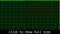
this is the push pull drive circuit and the results for my own circuit. Is this the way to do it?
 

Attachments

  • Untitled.png
    Untitled.png
    28 KB · Views: 156
  • 1.png
    1.png
    41.3 KB · Views: 162
  • 2.png
    2.png
    33.7 KB · Views: 156
  • 3.png
    3.png
    37.1 KB · Views: 141
  • 4.png
    4.png
    41.7 KB · Views: 135
Last edited:

In the half-bridge circuit, the IR2112 bootstrap supply istn't wired correctly. VB must not be shorted to VC, a diode is needed here. Compare with the application circuit in the datasheet.
 
Thanks Fvm. I had corrected the circuit but the Vg1 seems lk having large peak voltage.


Seriously, I can't comment the waveforms without seeing a corresponding circuit. To visualize the high-side transistor operation, you may want to plot Vgs rather than Vg.
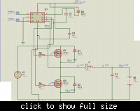
 
Seriously, I can't comment the waveforms without seeing a corresponding circuit. To visualize the high-side transistor operation, you may want to plot Vgs rather than Vg.

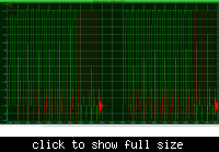
Yea, it should be Vgs and now i get the results. Thank you very much. You really help me a lot.


---------- Post added at 10:00 ---------- Previous post was at 08:06 ----------

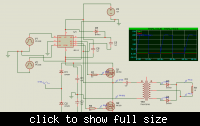
Now I try to put the driver circuit into another circuit which is going to be a half bridge converter. I canceled out the transformer part because I couldn't run it. So I only attached the first part of the circuit. The output Vgs1 behaves very weird and has a high values.


IR2112 COM must be connected to the source of the low-side transistor respectively the negative bus voltage terminal.Notice the two ground symbols in your circuit!
 
Sorry, I thought COM is connected to the ground. I think this is the correct connection. Actually, I want to make this circuit to become half bridge converter, so I would like to ask is it only the upper mosfet on during positive cycle and lower mosfet on during negative cycle. Now my attached circuit, the lower mosfet is connect to a capacitor before going to ground. So, will it cause any problem to the Vgs2 as it does not directly connect to ground. I also set my pulse frequency into 100Hz so that each will on each half cycle. But the Vgs1 and Vgs2 are very high values.
 

Attachments

  • 1.png
    1.png
    108.7 KB · Views: 136
  • 2.png
    2.png
    56 KB · Views: 134
Last edited:

Theer are several details, that can't be neither seen from the circuit nor from the waveform. So I simply can't determine if something's wrong and what it is. One thing, that is surely wrong is the ground connection of the IR2112 SD terminal. The IR2112 COM pin must also be connected to the gate driver supply (D5) ground and the common ground of the control input. And I can't see how Vgs1 and Vgs2 are measured.
 
that is surely wrong is the ground connection of the IR2112 SD terminal
From the data sheet, it states that SD is logic input for shutdown. What does this mean? Do I really need to put input to SD?

the IR2112 COM pin must also be connected to the gate driver supply (D5) ground and the common ground of the control input.
Yea, now my Vgs1 and Vgs2 become normal pulse. Thank you very much. But I still don't understand why the COM pin need to be connected to the gate driver supply and common ground of the control input? Since in #11, for the dc chopper, i did not connect the COM pin to the connected to the gate driver supply and common ground of the control input. I still can obtain the results.


And I can't see how Vgs1 and Vgs2 are measured.
Vgs1 = R2(2)-Q1(s)
Vgs2 = R3(2)-Q2(s)
 

In the new circuit (#17), you're shorting C2, because you have a ground symbol at both of it's both sides. The IR2112 requires the negative bus voltage to be connected to common ground (logic and gate driver supply ground), than you can't connect it to mid supply simultaneously. It's easy to solve the problem in a simulation, but you should know, how you want to design a real circuit.

I'm sure, you have a connected logic and gate driver supply to common ground in circuit #11 as well, otherwise, the supply would be floating.
 
Thanks Fvm. Now I change the circuit into half bridge converter without the filtering. The result does not show a full wave rectification. I think the problem starts at the beginning of the circuit because during negative cycle, there is no waveform coming out. Is it due to the grounding at the capacitor?


You are still shorting C2 by placing ground symbols on different nodes. It can't work this way! See my correction below:

 
Status
Not open for further replies.

Part and Inventory Search

Welcome to EDABoard.com

Sponsor

Back
Top