sebmaster
Member level 1

Hi,
I want to build an array of ~60 current limiter (500mA) circuits to act as power sources. In normal operation, they will basically be electric fuses (i.e. the expected current is < the design/limited current). So, the current limiting does not have to be incredibly accurate, and cost and size are important.
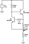
I found this circuit online, but wondered if someone could check my calculations for the components, to make sure I have reasoned them correctly, and not missed anything?

I have worked it out as follows, assuming the worst case scenario (a short across the load):
Q1
The pass transistor is a 2STD1665 because it is high power, has a low Vce, is cheap and supplied in small quantities.
Thermal Dissipation
Design current is 500mA at 12v, so 6W.
+30% safety margin is 8W.
The 2STD1665 has a Junction-Ambient Thermal Resistance of 8.33 C\W and a max junction temp. of 150 deg.
At 8W that is a temp. rise of 66 degrees, giving a max. ambient. temp of 83 degrees, so no heatsink is required.
Rbias
Ib1 should be hfe*design current (0.5A) = 0.005A (actual hfe is larger, so we have headroom)
Vrbias should be Vcc - Vbe1 - Vrsense. Vbe1 is 0.85-1v, and Rsense is 0.7, so Rbias = ~10V / 0.005A = 2kohm.
Q2
Q2 only has to pass Irbias (5mA) so can be any NPN such that it (Ic2) handles this, and Vce2 < Vbe1. (e.g. BC847: Vce < 0.4)
R1
R1 protects Q2 in case the full Vcc appears across Rsense. I asked about this on another site and don't believe its essential in any conditions I can think of (that don't blow up a lot more than Q2), but since it is negligible to include, and covers conditions I can't think of, I am including it.
Vcc - Vce is ~11.9V, so R1 should be 120ohm.
Rsense
RSense actives Q2 when the current across it creates a voltage drop greater than Vce. I assume Vce is ~0.7. R1 and Q2 form the equivalent of a diode resistor pair, in parallel with Rsense. So it is strictly calculated as:
0.7 + Ib2*R1 = 0.5 * Rsense
Though at the design current when Q2 switches, Ic2 = 0.005, so Ib2 = 0.00005, so Ib2*R1 is ~0.006ohm which is <1% of Rsense, so it can effectively be ignored.
This leaves Rsense = 0.7/0.5 = 1.4ohm.
Have I gone about that the right way?
Sj
I want to build an array of ~60 current limiter (500mA) circuits to act as power sources. In normal operation, they will basically be electric fuses (i.e. the expected current is < the design/limited current). So, the current limiting does not have to be incredibly accurate, and cost and size are important.
I found this circuit online, but wondered if someone could check my calculations for the components, to make sure I have reasoned them correctly, and not missed anything?

I have worked it out as follows, assuming the worst case scenario (a short across the load):
Q1
The pass transistor is a 2STD1665 because it is high power, has a low Vce, is cheap and supplied in small quantities.
Thermal Dissipation
Design current is 500mA at 12v, so 6W.
+30% safety margin is 8W.
The 2STD1665 has a Junction-Ambient Thermal Resistance of 8.33 C\W and a max junction temp. of 150 deg.
At 8W that is a temp. rise of 66 degrees, giving a max. ambient. temp of 83 degrees, so no heatsink is required.
Rbias
Ib1 should be hfe*design current (0.5A) = 0.005A (actual hfe is larger, so we have headroom)
Vrbias should be Vcc - Vbe1 - Vrsense. Vbe1 is 0.85-1v, and Rsense is 0.7, so Rbias = ~10V / 0.005A = 2kohm.
Q2
Q2 only has to pass Irbias (5mA) so can be any NPN such that it (Ic2) handles this, and Vce2 < Vbe1. (e.g. BC847: Vce < 0.4)
R1
R1 protects Q2 in case the full Vcc appears across Rsense. I asked about this on another site and don't believe its essential in any conditions I can think of (that don't blow up a lot more than Q2), but since it is negligible to include, and covers conditions I can't think of, I am including it.
Vcc - Vce is ~11.9V, so R1 should be 120ohm.
Rsense
RSense actives Q2 when the current across it creates a voltage drop greater than Vce. I assume Vce is ~0.7. R1 and Q2 form the equivalent of a diode resistor pair, in parallel with Rsense. So it is strictly calculated as:
0.7 + Ib2*R1 = 0.5 * Rsense
Though at the design current when Q2 switches, Ic2 = 0.005, so Ib2 = 0.00005, so Ib2*R1 is ~0.006ohm which is <1% of Rsense, so it can effectively be ignored.
This leaves Rsense = 0.7/0.5 = 1.4ohm.
Have I gone about that the right way?
Sj


