Continue to Site

Welcome to EDAboard.com

Welcome to our site! EDAboard.com is an international Electronics Discussion Forum focused on EDA software, circuits, schematics, books, theory, papers, asic, pld, 8051, DSP, Network, RF, Analog Design, PCB, Service Manuals... and a whole lot more! To participate you need to register. Registration is free. Click here to register now.

[SOLVED] h-bridge simulation ugly signals

Status
Not open for further replies.

d123

Advanced Member level 5
Joined
Jun 7, 2015
Messages
2,505
Helped
494
Reputation
992
Reaction score
525
Trophy points
1,393
Location
Spain
Activity points
27,148
Hi,

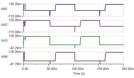
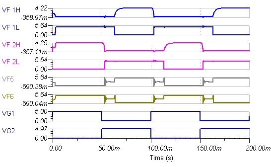
At first glance does anyone recognize what the cause of the horrible h-bridge signals (VF5 and VF6) are being caused by? I put plenty of dead-time in there, as can be seen from the immaculate gate signals, 1H + 1L and 2H + 2L - nothing coincides where it shouldn't and what has to be off is off and what has to be on is on at their expected times. How can there be shoot-through when e.g. T1 and T3 never coincide in being on? I assume it's something obvious and I'm being thick not understanding what I'm being shown by the simulation. Either I can't see something I should by now or I don't understand what ugly 5 and ugly 6 mean here. VG1 is 10 Hz, the inductor has 40 Ohms of resistance, fwiw as information. I'm probably really trying to learn about implementing dead-time and assorted configurations that can achieve that, not making a discrete h-bridge.

Thanks.
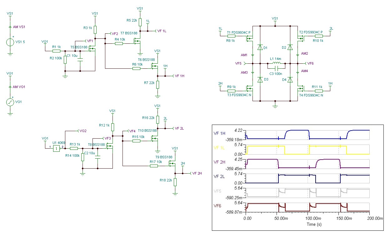
a bridge v1 schematic.JPG


a bridge v1 transient 3 current.jpg


a bridge v1 transient 4 voltage.jpg
 

Hi,

1k Ohm gate resistance is much too high.
and the 22k to sssslllloooowwwwlllyyy discharge gates makes it worse.


Klaus
 
  • Like
Reactions: d123

    d123

    Points: 2
    Helpful Answer Positive Rating
You will hardly be able to implement the gate driver delay with just one transistor stage, it is necessary a saturation circuitry somewhere; you could rather consider a Schmitt trigger arrangement, or since you are supplying the logic with 5V, you could simply replace the 4 MOSFET's with a single IC gate ( e.g 4000 series ) instead.
 
  • Like
Reactions: d123

    d123

    Points: 2
    Helpful Answer Positive Rating

    c_mitra

    Points: 2
    Helpful Answer Positive Rating
Hi,

may I ask what´s the idea behind this circuit?
Why build such a circuit and what is it used for?

My thougths:
* .. because there is no "ready to buy" solution. But I guess there is.
* .. because it´s cheaper than the "ready to buy" solution. But if you take all the effort and parts into account...
* .. it has some benefits against the "ready to buy" solutions. I don´t see..

Especially the big capacitors C1, C2 do not only delay the signal, they cause low rise and fall rate.
But this low rise/fall rates cause high power dissipation during switching (switching loss). So while the MOSFETS with their low R_DS_ON generate low heat when ON (conduction loss) but maybe much more swtiching loss.

When driving inductive loads you may avoid DC in the ouput signal. Due to capacitor (and other components) tolerance one side may be faster than the other ... unsymmetric timing, which may cause unwanted DC.

Even if you want to build your own circuit I recommend to read through some "ready to buy" parts datasheets and according application notes. To find out and avoid the pitfalls.

Klaus
 
  • Like
Reactions: d123

    d123

    Points: 2
    Helpful Answer Positive Rating
Hi,

I was just exploring implementing dead-time. Maybe to make a 'clock' that never moves forward in time, just one tick forwards and one tock backwards forever; it would need to be with a stepper motor anyway, not the 'motor' in the schematic, so the drive circuitry would be different. Main interest was wave shaping for dead-time and an h-bridge seems a good circuit to see if that is working correctly or not. Apart from what you mention about avoidable switching losses I see it's a flawed design, anyway, previous comments drew my attention to a couple of important design aspects - the VF1 from the VG1 signal needs to be turned off before the VF2 from the VG2 one starts (and vice versa) as well as turning off the bridge MOSFETs far faster. Bad design.
 

  • Like
Reactions: d123

    d123

    Points: 2
    Helpful Answer Positive Rating
Status
Not open for further replies.

Similar threads

Part and Inventory Search

Welcome to EDABoard.com

Sponsor

Back
Top