Continue to Site

Welcome to EDAboard.com

Welcome to our site! EDAboard.com is an international Electronics Discussion Forum focused on EDA software, circuits, schematics, books, theory, papers, asic, pld, 8051, DSP, Network, RF, Analog Design, PCB, Service Manuals... and a whole lot more! To participate you need to register. Registration is free. Click here to register now.

[SOLVED] H-bridge driving problem,MOSFET frequently damage

Status
Not open for further replies.

Mithun_K_Das

Advanced Member level 3
Joined
Apr 24, 2010
Messages
899
Helped
24
Reputation
48
Reaction score
26
Trophy points
1,318
Location
Dhaka, Bangladesh, Bangladesh
Activity points
8,254
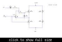
I'm using H-bridge with IRF740 (MOSFET) to convert 315VDC to 230VAC. But the upper mosfets are frequently get damage within few seconds. I can't find what is the problem. Help me...
 

My first suggestion to help would be to use a normal size font, we can read it fine.
Your circuit may have an improper mosfet driver or the problem can be coil back emf related but as FvM said post your circuit instead of having us guessing.

Alex
 
Last edited:

so you are using the mosfets without proper drivers, 1K for the gate of the upper mosfer and 10k for the lower mosfet, this means slow switching speed.
Also the 13001 transistor has a strange operation, it discharges the upper mosfet gate when the lower mosfet turns on, I 'm not sure that you have a proper dead time between switching sides.
In order for the transistor to work and discharge the upper mosfet gate the lower mosfet has to be on first to provide the ground so there is a time where both of them are on.

Another note is that to turn on the Nmosfet you need about 10v (Vgs) to have a low Rds-on but in your upper mosfet you have the diode ( D2 ) which doesn't let the gate have more than 0.7v compared to the source and this will overheat the mosfet.

Alex
 

Looks like a failed attempt to design a bootstrap driver. The circuit, as shown, will operate the high-side transistors as source followers and can't turn it on. High losses will quickly damage the transistors if any load is connected. In some situations, e.g with inductive load, also the driver transistor and low side transistor will be blown.

It's not completely impossible to design a discrete bootstrap driver, but it will be considerably more complex than your circuit. You better use an industry standard driver IC instead.
 

can you give any circuit diagram? I've been in trouble in this section only for a long time. This is just a part of my thesis. please help.


Oh! that was my mistake to draw quickly to post. anyway thanks.

---------- Post added at 14:58 ---------- Previous post was at 14:53 ----------

78_1305554167.jpg


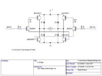
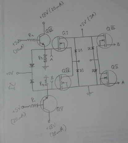
I found these 2 circuits. how about them? will they work?
 

None of these circuits will work with high DC bus voltages. A standard bootstrap driver as IR2110 can.
 

if I replace the transistors/mosfets with HV ratings, then?

---------- Post added at 15:45 ---------- Previous post was at 15:20 ----------

datasheet of IR2110 says that the IC have to run at 15V Vcc, but I'm working with 12V Vcc and logic TTL. so how can I use IR2110?
 

if I replace the transistors/mosfets with HV ratings, then?
I don't see a reasonable way.
datasheet of IR2110 says that the IC have to run at 15V Vcc, but I'm working with 12V Vcc and logic TTL. so how can I use IR2110?
The key specification can be found on the very first lines of the datasheet, titled "Features".
Gate drive supply range from 10 to 20V
3.3V logic compatible
5V is actually better for low delay.
 

Vcc is the voltage used for bootstrapping, can be 10-20v, 12v is fine.
Vdd is the positive supply of the logic circuit, if you are using 5v mcu connect to 5v, if you are using 3.3v connect to 3v3.
Vss goes to the input ground and COM to the output ground.
The datasheet is quite clear on the voltage ranges that can be used, 15v VCC is just a typical example.

Alex
 
The upper high side driver in the IR2110 rides up and down the high voltage supply (315v). The power supply filter cap on this high side driver section drives the high side MOSFET driver circuitry. It is also known as the bootstrap cap. It is recharged every cycle when the low side MOSFET conducts on bottom side and through a diode that connects to the 12v supply on high side of cap. This give approximately 10 to 11 vdc charge (12v - diode drop - Vds ON of lowside MOSFET). You must have switching periodically on the low side MOSFET to refresh the charge on the high side bootstrap cap. The IR2110 will not operate in a static drive condition (like fixed, full speed motor reversing).

The input logic goes to a current source drive to high side driver that has a high voltage breakdown limit so the high side driver section can ride 'up in the air' to the high side voltage (315v + 10v in your case). The driver will drive the gate of the high side MOSFET 10 vdc above the 315 vdc supply to ensure the high side Nch MOSFET is put into full conduction.

Attached is a schematic with a discrete high side MOSFET driver. The BJT devices must have a breakdown voltage higher then the high voltage on the high side MOSFET's.
 

Attachments

  • power_inverter_300w.pdf
    135.3 KB · Views: 396
Last edited:
many many thanks to RCinFLA. I've got this circuit in a China product, 600W/12V inverter. I was trying to find out the schematic diagram from their product.

---------- Post added at 18:09 ---------- Previous post was at 18:05 ----------

I can't understand the function of D6 & D7. can you explain? this circuit is for 155V, my one is 315V.
 

I agree, that the driver presented by RCinFLA can work for a low frequency switcher, e.g. 50 or 60 Hz square wave inverter. But is has some weaknesses:
- it's switching rather slow (10 µs range)
- unlike an IR2110 it hasn't an undervoltage lockout. If the bootstrap capacitor isn't correctly charged, the high side driver can operate in linear mode and may be quickly damaged.

I fear, the circuit is simple but not easy to implement.
 

many many thanks to RCinFLA. I've got this circuit in a China product, 600W/12V inverter. I was trying to find out the schematic diagram from their product.

---------- Post added at 18:09 ---------- Previous post was at 18:05 ----------

I can't understand the function of D6 & D7. can you explain? this circuit is for 155V, my one is 315V.

To provide DC to run LED active indicator (it's an LED not an incandescent bulb).

This inverter is like 20+ years old. It is a modified sinewave inverter. Another issue is the DC-to- HVDC inverter has no isolation on its feed backpath. This makes the neutral side of AC ungroundable and often makes equipment plug into inverter have slight 'live chassis' getting a bit of a tingling shock when touching metal on plug in equipment case.

Using a IR2110 or other similar driver IC's are only way to go these days.
 
Last edited:

both of you (FvM & RCinFLA) making me confused. Please tell me what should I chose? I'm using atmega8 as the main controller of my circuit. and also generating a sine wave using this mcu to get a sine wave output. so, which one will be best for me?
 

The recommendation have been pretty clear.

In addition, if you intend PWM operation, which is the only reasonable way to achieve sine output in my opinion, switching speed will be an issue. Low impedance push-pull gate drivers are absolutely required in this case.
 

Status
Not open for further replies.

Similar threads

Part and Inventory Search

Welcome to EDABoard.com

Sponsor

Back
Top