Continue to Site

Welcome to EDAboard.com

Welcome to our site! EDAboard.com is an international Electronics Discussion Forum focused on EDA software, circuits, schematics, books, theory, papers, asic, pld, 8051, DSP, Network, RF, Analog Design, PCB, Service Manuals... and a whole lot more! To participate you need to register. Registration is free. Click here to register now.

H-Bridge burns out from one side without load (Randomly)!

Status
Not open for further replies.

HelpMe2020

Newbie
Newbie level 1
Joined
Feb 24, 2021
Messages
1
Helped
0
Reputation
0
Reaction score
0
Trophy points
1
Activity points
28
Hello All,

I am new to the community and this query would be my first post on the forum. So, apologies in advance if I not strictly adhering any guidelines.

I have designed this H-Bridge and corresponding PCB was also fabricated. I simulated it on LTSpice, too. It has two variations with +12V and +24V supply. I have tested it and it has been working fine driving various DC motors. However, sometimes (randomly and sporadically on both +12V and +24V) with no load i.e no motor connected, the one side of H-bridge (both P-MOSFET and N-MOSFET) would fry out together very bad, and then those two MOSFETs are actually gone bad. I'd replace those two MOSFETs with new ones and it would start working again. Next time, randomly, other side would burn out. However, I never saw it failing or heating out whenever it starts working once and load is connected. It would work seamlessly. It randomly fries out only when no load is not connected. (Always right away when I insert +12V or +24V supply into it --> Again, randomly burns out). It would fry out right away after voltage supply is inserted if it has to otherwise it wouldn't. It never fries once the voltage is provided and circuit is stable. It would fry only randomly and immediately when +12V/+24V supply is inserted. Could this be random inrush current? Could this be mismatch of Rds? Let me re-emphasis that both the MOSFETS from one side fries out together.

Please recommend changes that might fix this solution. Any recommendation will be greatly appreciated!

Note: The above experience happened when M1 and M2 were AOD4189. I have changed the P-MOSFETs to the new ones (IPD068P) with matching Rds that of IRLR8726 to avoid shoot-through. I haven't tested the changes. I want to be double sure that I am not missing something else.
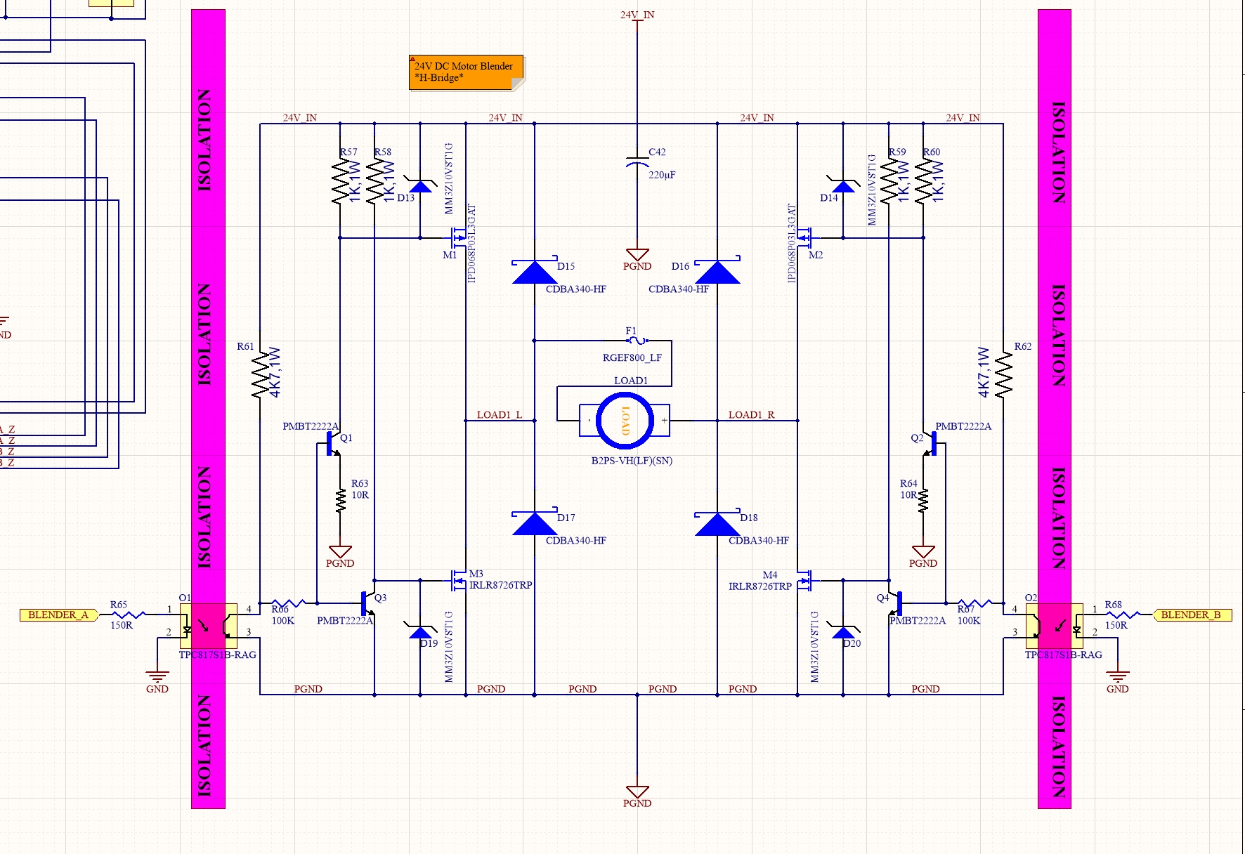
Screenshot 2021-02-24 at 12.58.06 PM.png
 

What voltage is applied to the mosfet gates when no load is present ? Shoot-through is the first possibility to examine.

To avoid unwanted turn-On it's common to pull the gate to source voltage by permanently installing a 10-20 k resistor between gate & source. The aim is to prevent the mosfet turning On when you don't want it to. If you leave the gate wire at high impedance then it can be influenced by stray static or EM interference.
 

Hi,

It's poor design.
Especially the combination of Q1/Q3 and Q2/Q4. Thermal drifts may lead to unwanted behaviour.
And the 100k of R66 is extremely high and may slow diwn signals during transitions.

The optocoupler outputs are pulled up rather low ohmic, about 5mA. Good for speed, but this maybe causes rather bad LOW levels. Then you try to drive two BJTs with just 0.2mA. This does not match. Less than 5% of the current is used to drive the next stage, 95% are wasted as heat.
And I miss an R_BE to safely and fast turn OFF Q1...Q4.

For sure it may work on "ideal" situations on a simulator (where all transistors have exactly same temperature and thus same V_BE), but reality is different.

Also you have to be sure that your design works reliably when the bus supply
* is switched ON before the logic
* is switched ON after the logic
* slowly rises
* slowly falls
And check what happens when the motor is on full speed and you
* immediately switch it OFF. Braking and/or non braking
* reverse the polarity
* switch OFF the power supply and the motor (with it's rotational energy) acts as a generator, pushing back electrical energy to the power bus.
Consider to include features like: overcurrent protection, undervoltage protection, overtemperature protection.

My recommendation:
There are probably million of proven circuits in the internet.
Most semiconductor manufacturers provide design notes for free how to design such circuits. They are very detailed and give very reliable results. They tell you the pitfalls and how to avoid them.
There are ready to buy motor drivers ICs, there are ready to buy motor driver modules.

I don't think it's a good idea to design this from the scratch - without having the experience and without reading related literature.
Building a switching full bridge motor driver is not a simple task, there are a lot of pitfalls. Even the PCB layout will have much influence whether the circuit will work reliably and satisfactory ... and last but not least it needs to fulfill regulations. Safety, EMI/EMC, environmental....

Don't get me wrong.
* I don't want you to stop to learn circuit design. If you have the time and money .. and can handle the fails ...
.. the fails that others already have experienced before. You are free to do...
* Instead I want to encourage you to learn circuit design. Use the internet. Learn to find and use reliable informations from semiconductor manufacturers, universities, reliable designers.. read documents, go through different approaches to learn the benefits and drawbacks, watch videos....

Klaus
 

I agree with Klaus but primarily I doubt Q1/Q3 and Q2/Q4 are behaving as you expect. With R66 being such a high value and the base-emitter junctions of the transistors being almost in parallel they probably are not switching hard on and off as they need to.

Personally, and keeping it simple, I would remove R63 and use say 1K from each base to the optocoupler. That should provide far more base current and prevent one transistor clamping the other.

Brian.
 

Hello All,

I am new to the community and this query would be my first post on the forum. So, apologies in advance if I not strictly adhering any guidelines.

I have designed this H-Bridge and corresponding PCB was also fabricated. I simulated it on LTSpice, too. It has two variations with +12V and +24V supply. I have tested it and it has been working fine driving various DC motors. However, sometimes (randomly and sporadically on both +12V and +24V) with no load i.e no motor connected, the one side of H-bridge (both P-MOSFET and N-MOSFET) would fry out together very bad, and then those two MOSFETs are actually gone bad. I'd replace those two MOSFETs with new ones and it would start working again. Next time, randomly, other side would burn out. However, I never saw it failing or heating out whenever it starts working once and load is connected. It would work seamlessly. It randomly fries out only when no load is not connected. (Always right away when I insert +12V or +24V supply into it --> Again, randomly burns out). It would fry out right away after voltage supply is inserted if it has to otherwise it wouldn't. It never fries once the voltage is provided and circuit is stable. It would fry only randomly and immediately when +12V/+24V supply is inserted. Could this be random inrush current? Could this be mismatch of Rds? Let me re-emphasis that both the MOSFETS from one side fries out together.

Please recommend changes that might fix this solution. Any recommendation will be greatly appreciated!

Note: The above experience happened when M1 and M2 were AOD4189. I have changed the P-MOSFETs to the new ones (IPD068P) with matching Rds that of IRLR8726 to avoid shoot-through. I haven't tested the changes. I want to be double sure that I am not missing something else.
View attachment 167753
Hi
Do you have enough dead time in your drive signals a and a' ?
Its also possible that gate sources being self charged somehow so adding a parallel damping resistor would probably solve it .
Btw : why you didnt use a float driver instead ? For instance ir 2113 or ir2110 or ... ?
 

No-load can be the highest dV/dt condition and
this could trigger burnout especially if gate drive
is not "stiff", or if the FETs chosen are prone to trigger
the parasitic BJT at high drain slew rates.

But I don't think that trying to turn off a FET with
5nC typ gate charge, using a 1K resistor, is going
to ever work out well. Probably quite a protracted
Miller plateau (the highly dissipative region which
you'd much rather get through, smartly).

Have you tried looking at the four gate signals to
see what sort of cross-conduction they might be
commanding in their legs? Waveforms trump any
speculation about causes.
 

Status
Not open for further replies.

Part and Inventory Search

Welcome to EDABoard.com

Sponsor

Back
Top