Continue to Site

Welcome to EDAboard.com

Welcome to our site! EDAboard.com is an international Electronics Discussion Forum focused on EDA software, circuits, schematics, books, theory, papers, asic, pld, 8051, DSP, Network, RF, Analog Design, PCB, Service Manuals... and a whole lot more! To participate you need to register. Registration is free. Click here to register now.

ground routing question

yefj

Advanced Member level 5
Joined
Sep 12, 2019
Messages
1,505
Helped
1
Reputation
2
Reaction score
5
Trophy points
38
Activity points
9,114
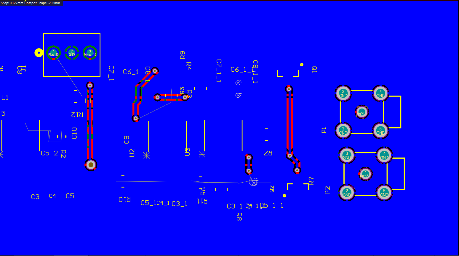
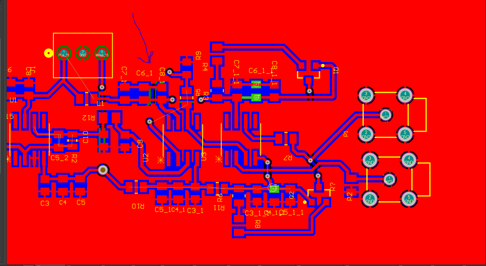
Hello,As you can see i have section of a circuit in which the traces of DC and traces of a signal pass threw bottom layer.
te problem is that is it passes threw buttom layer it needs a solid GND layer on the top layer and in the section shown i the blue arrow i dont have much GND for the little section of trace shown below in the arrow.
How do i know if it will cause problems?
what are the alternatives?
Thanks.

Top layer:
1708853007306.png

Buttom layer:
1708852795717.png
 
Your PCB has almost no connections between top and bottom ground copper. Why? You should treat the combination of both as meshed ground, with sufficient stich vias all over the board. This way you can easily bridge discontinuity of bottom ground.
 

    yefj

    Points: 2
    Helpful Answer Positive Rating
Hi,

for me: the top GND is not important at all. I relate to the bottom GND.
TOP GND is usually never solid, it is cut into pieces with rather high imedance betwenn those pieces.
Thus I rarely use GND pour at TOP layer.

In your case, why not move R5 and R9 left of U3?

As FvM said ... you have a nice solid BOTTOM GND layer ... but you don´t use it.
Thus all your GND loops become huge. High impedance, not suitable for HF. Bigger EMI/EMC problems.


Klaus
 
Hello Klaus, FVM said I need to put stitching Via's as a solution.
do you agree that it will solve my huge gnd loop problem and my signal traces on the buttom layer will have sufficient GND from top layer?
Thanks.

1708856923548.png
 
As said: I almost never use GND pour at TOP, I always relate to the BOTTOM GND .. and the only ways is to use vias (sometimes multiple) next to each part_GND_pin directly down to the bottom layer.

Stitching vias are needed if you want use TOP layer GND pour and you want to connect these to the bottom GND.

In post#1 you say "solid GND layer on the top layer", but you have to accept that you TOP GND is far from being "solid". Your BOTTOM GND is solid.

Klaus
 
Hi,

I agree with @KlausST I would consider the BOTTOM GND layer as the important one as well, especially if the system frequency if high. I assume youe signal frequncy is "high" as I see two SMA (?) connectors used in your design. For "high" frequencies, the return current path is the one with the lowest impdance (not resistance) and this will be the BOTTOM GND plane in your desing if GND-VIAs are placed next to the GND pad of the components. The return current will flow under the source/input-trace if possible, to create a small loop, which means a low impedance. Just have a look on your TOP GND plane, here it is not that easy for the return current to travel next to the source/input-trace. This will create larger current loops, and consequently a larger impedance.

BR
 
Hello ,I have addred stiching VIAS between the layers.
actually its not HF but almost DC signal going in.
my only concern is noise and stability up to 5Mhz.
given the schematics below could you recommend me a new stack up where there will not be such problem?
Thanks.
1708868468135.png


1708867575466.png

1708867670883.png

1708867700377.png

--- Updated ---

Update:

Hello, this is my bare PCB schematics .do you suggest that placing R5 and R9 on the bottom layer will be better?
if so how do you recomend to place R9 and R5?
my opamp is on the top level and the components are on the bottum,what is the optimal way to do it?
Thanks.

1708871880658.png
 
Last edited:
Why are you still using 3 Op Amps with the bandaid current sensing BJT amplifiers when you can get far better performance from one Op Amp?
1708916626396.png

What are your final present design specs?

This isn't even UHF in spectrum.
Also your coax output capacitance from the current source creates a resonant circuit with high Q inductive load, so if necessary, include in spec.

I don't think your design isn't ready to layout.
 
Last edited:
Hello,Klaus gave a very good advice which I think i found in other place too but i cant understand how do i recognize this situation i PCB.
Could you give a practical example where i could see this effect mathematically?
Thanks.


Hi,

for me: the top GND is not important at all. I relate to the bottom GND.
TOP GND is usually never solid, it is cut into pieces with rather high imedance betwenn those pieces.
Thus I rarely use GND pour at TOP layer.

In your case, why not move R5 and R9 left of U3?

As FvM said ... you have a nice solid BOTTOM GND layer ... but you don´t use it.
Thus all your GND loops become huge. High impedance, not suitable for HF. Bigger EMI/EMC problems.


Klaus
1708949840315.png
 
Regarding Parasitic Oscillations from layout can be simulated by lumped elements.
Here using 3 pF with 100 pF coax to load.


Coplanar traces use the height as the electrode facing each other, so C is much smaller even if closer than substrate depth. Also Dk =1 above the trace. Yet in high current SMPS and RF pwr amps top side is useful for heatsink and EMC improvement. Interleaved ground tracks are usually adequate to avoid crosstalk.

You can model the trace capacitance for interference as well as he same signal using lumped elements.

I hope this attempt to visualize the effects of positive and negative feedback works.

Assumptions:
Howland Current Sources for broadband use with 1m of coax = 100pF to 50 Ohms load.
Ideal Op Amp: with infinite BW internally compensated, no current limit, Aol =100 dB gain, Ideal supplies = +/-15V

If there is any coupling of positive feedback from out to in, it can be corrected with negative feedback.
Otherwise there will be parasitic oscillations stimulated by transitions. (high Q spectral amplification)
1708967201798.png
 
Hi,

some problems I see with this thread:
* The OP is not able to focus on one problem, discuss this problem, solve this problem, step to the next problem.
* the given informations don´t match: text vs schematic vs PCB layout.

Especially the mismatch between schematic and PCB layout is what I don´t understand. Every layout software should have forward and back annotation in a way that both stay consistent. Thus I guess the mismatch is not caused by the software.
This "not matching" causes confusion, misunderstandings and is time consuming.

* Schematic as is has it´s problems, but may work,
* but the (schematic of the) PCB circuit makes no sense at all.

I´m out.

Klaus
 
Hello,I dont understand the link between routing and impedance and loop.
Is there some example i could use to understand th issue in PCB?
What is the link between the loops and impedance.


for me: the top GND is not important at all. I relate to the bottom GND.
TOP GND is usually never solid, it is cut into pieces with rather high imedance betwenn those pieces.
Thus I rarely use GND pour at TOP layer.
--- Updated ---

UPDATE:
I know i need my PCB to function as situation A.
How do i know that i am at situation B?

1709020186939.png
 
Last edited:
Hello,Klaus gave a very good advice which I think i found in other place too but i cant understand how do i recognize this situation i PCB.
Could you give a practical example where i could see this effect mathematically?
Thanks.
Do you have any PCB/EMC tools? Even Saturn PCB (free) will show you the CONDUCTOR IMPEDANCE for top layer (microstrip) with capacitance and inductance for any Er and f. Learn how to use Saturn PCB impedance tools and checkout their physics references.
Using microstrip traces which share air and FR-4 at low rise time and low W/H you can see what you have for traces over ground.

Again, I believe it would be a mistake to interface this Howland Current Source to an inductive load on a long coax. with ~1.23 pF/cm. = 123 pF/m

Then you can see top traces share air on one side and FR-4 on the other means that trace only see about 63% of the Er (epsilon-R) for a std FR-4 board < 100 MHz
The SINGLE GND PLANE trace capacitance is 0.0392 pF/mm to ground. In your layout it is not significant compared to coaxial shunt capacitance ~100pF/m and remote ground noise injection.

But as I demonstrated in my simulations the distributed LC elements can identical to lumped LC's parts.

At these low frequencies you have no issues with positive feedback crosstalk for spurious oscillations, but you may have unacceptable consequences to inductive servo coil load, excess coaxial cable capacitance and remote ground noise.
 

LaTeX Commands Quick-Menu:

Similar threads

Part and Inventory Search

Welcome to EDABoard.com

Sponsor

Back
Top