Continue to Site

Welcome to EDAboard.com

Welcome to our site! EDAboard.com is an international Electronics Discussion Forum focused on EDA software, circuits, schematics, books, theory, papers, asic, pld, 8051, DSP, Network, RF, Analog Design, PCB, Service Manuals... and a whole lot more! To participate you need to register. Registration is free. Click here to register now.

Ground pins set up in EM simulation for RFIC inductor

Status
Not open for further replies.

anh56789

Junior Member level 2
Joined
Jul 27, 2023
Messages
20
Helped
0
Reputation
0
Reaction score
0
Trophy points
1
Activity points
227
Hi,
I want to evaluate the performance of the inductor with the effect of the ground shielding similar to this post: https://muehlhaus.com/support/rfic-em-appnotes/inductor-ground-cutout
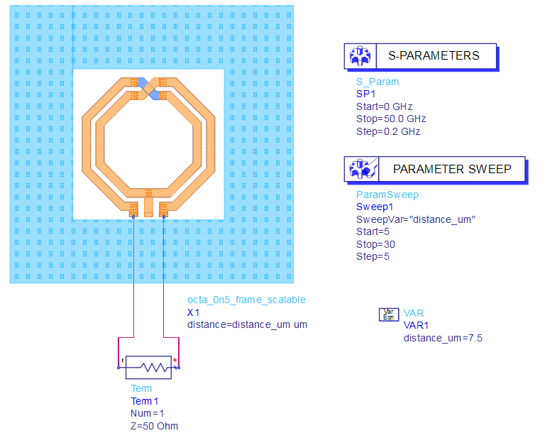
But I'm confused about how to define the voltage for grounding metal around the inductor. Below is the inductor test bench of the post
Inductor_testbench.png

In the test bench, I don't see any pin connected to the surrounding metal. So how could we know that the metal is connected to the ground? Is it a floating metal?
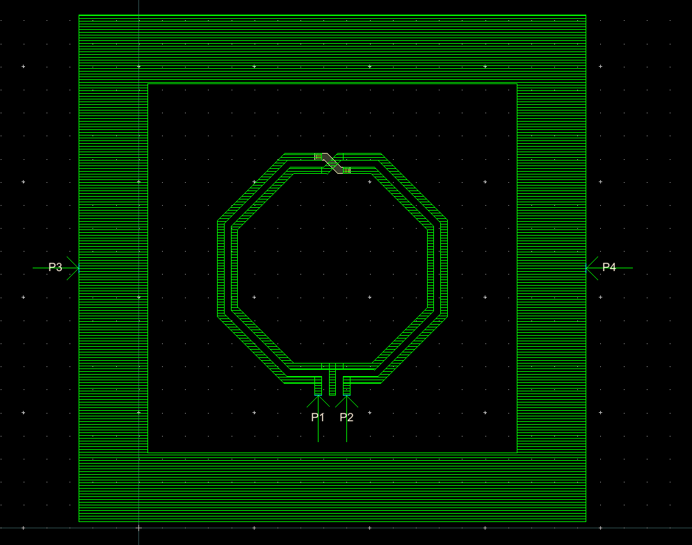
What if I want to use a port to define the GND for the surrounding metal? below is a picture of my layout. In this layout, I use ports 3 and 4 for defining the voltage of the surrounding metal.
Screenshot 2023-08-03 135520.png

Is it the correct way to set up the ground for the surrounding metal? Any insights on this problem would be appreciated. Thank you!!!
 

Solution
Is it a floating metal?
Yes, metal is floating in my example that you showed. The effect of that metal on Q factor shown there is an eddy current flowing around the cutout, and no port is required to show/model this.

If you want to put the ground plane at defined voltage, or model a patterned ground shield underneat the inductor, you can place a single port there. All ports, inductor and metal shield, can keep their ground reference at default global ground = bottom of the substrate. This way, you can still evaluate the shunt effects from inductor to the substrate node. The actual (circuit) connection is then made at schematic level using the 3-port data (or 4-port data if you have an additional port at inductor center...
You have to define a VIA in ADS then you should place this via around the coil in multiple numbers.
VIA : Metal To GND.
 

You have to define a VIA in ADS then you should place this via around the coil in multiple numbers.
VIA : Metal To GND.
Hi BigBoss,
Thank you for your quick response!
I think that will make the simulation results become unreliable because, in CMOS technology or SiGe, the VIA from TOP metal to GND doesn't exit. Below is the cross-view of the metal layer that I used in CMOS.
metal_scheme.png

As you can see in the picture, I use a perfect conductor at the bottom as a reference pin for EM ports. But in reality, we don't have that layer. The GND of the chip must come from PADs, and travel on top metal to sub-circuits. So I don't think using VIA from top metal to GND will be the solution. Am I right? Did I miss something?
 

No problem. The chip should have a GND connection either thru a PAD or in a different way.
You can use existing VIAs then model the GND connection of the chip. Don't forget to model the PAD with realistic ESD Diodes, internal GND connection, Bonding wires etc.
I must confess that this will impact the simulation but you wanna turnaround the coil and this will be a bit troublesome.
 

Is it a floating metal?
Yes, metal is floating in my example that you showed. The effect of that metal on Q factor shown there is an eddy current flowing around the cutout, and no port is required to show/model this.

If you want to put the ground plane at defined voltage, or model a patterned ground shield underneat the inductor, you can place a single port there. All ports, inductor and metal shield, can keep their ground reference at default global ground = bottom of the substrate. This way, you can still evaluate the shunt effects from inductor to the substrate node. The actual (circuit) connection is then made at schematic level using the 3-port data (or 4-port data if you have an additional port at inductor center tap).

edit: The single port for ground metal frame enables you to measure capacitance from inductor to that ground. However, that ground will not be included in the inductor current path, because port grounds are all at "global" ground.
If your goal is to also include current path through that ground path in results, you can indeed place one reference pin ("minus") for each inductor pin ("plus") instead of using global ground port reference at the bottom of the substrate. It really depends what you want/need to model, the "pure" inductor or some layout extract consisting of inductor and additional routing (here: current path in ground layer).
 
Last edited:

Solution
Yes, metal is floating in my example that you showed. The effect of that metal on Q factor shown there is an eddy current flowing around the cutout, and no port is required to show/model this.

If you want to put the ground plane at defined voltage, or model a patterned ground shield underneat the inductor, you can place a single port there. All ports, inductor and metal shield, can keep their ground reference at default global ground = bottom of the substrate. This way, you can still evaluate the shunt effects from inductor to the substrate node. The actual (circuit) connection is then made at schematic level using the 3-port data (or 4-port data if you have an additional port at inductor center tap).

edit: The single port for ground metal frame enables you to measure capacitance from inductor to that ground. However, that ground will not be included in the inductor current path, because port grounds are all at "global" ground.
If your goal is to also include current path through that ground path in results, you can indeed place one reference pin ("minus") for each inductor pin ("plus") instead of using global ground port reference at the bottom of the substrate. It really depends what you want/need to model, the "pure" inductor or some layout extract consisting of inductor and additional routing (here: current path in ground layer).
Hi Volker,
Thank you for your response!
Your explanation helped me understand better. I did simulate the inductor with the metal frame connected to the ground. Here is my test bench and results.

series_ind_with_diff_gnd_setup_results.PNG
series_ind_with_diff_gnd_setup.PNG


The spacing from the inductor to the metal frame is 30um. So that the Inductance and Q factor does not change so much. But there is still a small difference. Then I simulated the inductor which has a terminal connected to the ground. Here is my test bench and results.
shunt_ind_with_diff_gnd_setup.PNG
shunt_ind_with_diff_gnd_setup_results.PNG

You can see from the results that the position of the ground pin significantly affects the performance of the inductor. The inductance changes about 50% from 262pH to 393pH (GND position 1 to position 3). So I have a few questions.
1. For the series inductor test bench, we see that the number of pin grounds affects the performance of the inductor. So how do we define the ground pins? (how many pins and pin size). I think in reality, it depends on the number of pad grounds that are supplied to the chip but I don't know for sure.

2. For the shunt inductor test bench, the question is quite similar, Which position should we choose to evaluate the performance of the inductance? Does it depend on the return current path of the shunt inductor? I think the metal path from the pad grounds to the metal frames needs to be included in the EM simulation. But again, I don't really know the correct way to do this.

Could you help me out with my questions? Any insights would be appreciated!!! Thank you so much!!!
 

In your shunt models, inductor current must also flow through the frame, to the location of the grounded port. Of course, these results will be different because the path length is different between the models.

For the series model, results are close and the difference is small compared to simulation error (meshing etc.) For practical purpose, any of these models will be fine. The difference is from different path length in the frame to reach the ground node.

So which model is "correct"? That really depends on your requirements, as I explained above. For tank circuits etc we usually want to extract the "pure" inductor response, and that is what we usually show as inductor values L and Q. But if you have a grounded inductor then indeed the path length to the actual ground might be included in your model, which changes L and Q of course.

In your equations, you have calculated single ended inductor values (L and Q valid if one terminal is grounded) and even that depends on the actual use of the inductor. If you use differentially it in a symmetric circuit, the differential L and Q measured between the terminals would be the better (more relevant) data.

So the "best" model decision really depends on the use of the data, and the actual current flow in your circuit.
 
Last edited:
In your shunt models, inductor current must also flow through the frame, to the location of the grounded port. Of course, these results will be different because the path length is different between the models.

For the series model, results are close and the difference is small compared to simulation error (meshing etc.) For practical purpose, any of these models will be fine. The difference is from different path length in the frame to reach the ground node.

So which model is "correct"? That really depends on your requirements, as I explained above. For tank circuits etc we usually want to extract the "pure" inductor response, and that is what we usually show as inductor values L and Q. But if you have a grounded inductor then indeed the path length to the actual ground might be included in your model, which changes L and Q of course.

In your equations, you have calculated single ended inductor values (L and Q valid if one terminal is grounded) and even that depends on the actual use of the inductor. If you use differentially it in a symmetric circuit, the differential L and Q measured between the terminals would be the better (more relevant) data.

So the "best" model decision really depends on the use of the data, and the actual current flow in your circuit.
I got it. Thank you so much!!!
 

Status
Not open for further replies.

Part and Inventory Search

Welcome to EDABoard.com

Sponsor

Back
Top