Continue to Site

Welcome to EDAboard.com

Welcome to our site! EDAboard.com is an international Electronics Discussion Forum focused on EDA software, circuits, schematics, books, theory, papers, asic, pld, 8051, DSP, Network, RF, Analog Design, PCB, Service Manuals... and a whole lot more! To participate you need to register. Registration is free. Click here to register now.

Ground Pad Soldering Issue

Status
Not open for further replies.

jimmykk

Full Member level 3
Full Member level 3
Joined
Oct 2, 2014
Messages
158
Helped
0
Reputation
0
Reaction score
1
Trophy points
1,298
Activity points
2,865
Hi
I encountered a soldering problem while soldering 2 wires to my PCB.
The hole on the top is for GND and the below one is for Power.
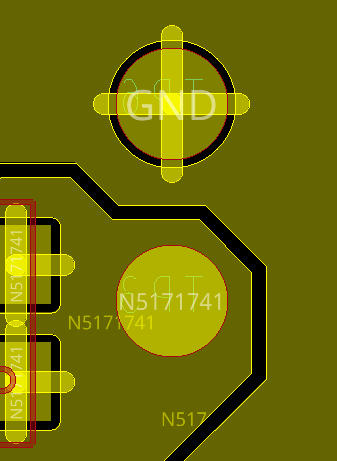
1685101422873.png

The wire is not getting properly soldered in the Ground Hole, while not much of a problem on the Power Hole.
The heat from the ground hole is getting spread over whole board and also, wire's insulation is melting.
To be honest, i was expecting the opposite. As the Ground hole has orthogonal connection which i assumed is
better for such type of soldering. Rather than Full Contact of Hole with surrounding Copper as in Power Hole.
 

Hi
I encountered a soldering problem while soldering 2 wires to my PCB.
The hole on the top is for GND and the below one is for Power.
View attachment 182970
The wire is not getting properly soldered in the Ground Hole, while not much of a problem on the Power Hole.
The heat from the ground hole is getting spread over whole board and also, wire's insulation is melting.
To be honest, i was expecting the opposite. As the Ground hole has orthogonal connection which i assumed is
better for such type of soldering. Rather than Full Contact of Hole with surrounding Copper as in Power Hole.
Hi,
it can be a problem in the Plated through holes .
the holes can be polluted or covered by solder resist partially during PCB production, which will cause poor solderability and connection with the wire after soldering.


Louis
 

That's a simple Thermodynamics issue with a larger ground plane to heat up.

- more Flux and heat with a properly cleaned tip. The PCB must not be oxidized from daily exposure. If so light pre-cleaning with abrasive pads. If still stubborn, pre-tin the pads with solder. If still a problem , show us a photo of your soldering tip.
 

Hi
Have encountered this issue over and over again that it is quite difficult to Solder a Wire or Connector to Through Hole Ground Pin
with orthogonal connection to the Surrounding Copper(Ground) Plane as shown here:
1688466606025.png

Top Layer connection is 0.2mm wide and Bottom Layer Connection is 0.4mm. Distance between Copper Pad and Plane is 0.15mm.
Through Hole Pin here has drill diameter of 1.5mm with annular ring of 0.25mm. That is 1.5mm hole with 2mm Copper Pad.
The wire won't just solder to this pin. I guess that all the heat dissipates to the surrounding Copper Plane immediately.

Would increasing the distance from 0.15mm to let us say 0.5mm would improve soldering and increasing the annular ring size?
 

I do not know the fill codes to dope out the layout but
a question is, whether there might be a center blind ground
plane that gets connected by the through-hole? Or a more
pervasive back side ground plane. If you can't get the pad
hot there must be a stout thermal path.

If you have a spare board to victimize, maybe set the iron
on that pad at max heat until "stuff" starts to char, and see
what that inkblot tells you about direction of heat flow. If
you have a thermal camera you could also use that. Take
pix of the one that works and the one that doesn't, in time
lapse series, and maybe you can follow the heat flux from
source to destination, and then break that thermal while
leaving the electrical path.

I do not believe the skinny cross is to blame but perhaps
there needed to be more gap, to lengthen the initial copper
path to the heat slab. You could probably do a thermal
impedance calculation from PCB vendor data, for the close-in
feature. But I think the real question is, "what's on the other
side of the gap, that you are missing?" for a heat sink.
 

Hi
I encountered a soldering problem while soldering 2 wires to my PCB.
The hole on the top is for GND and the below one is for Power.
View attachment 182970
The wire is not getting properly soldered in the Ground Hole, while not much of a problem on the Power Hole.
The heat from the ground hole is getting spread over whole board and also, wire's insulation is melting.
To be honest, i was expecting the opposite. As the Ground hole has orthogonal connection which i assumed is
better for such type of soldering. Rather than Full Contact of Hole with surrounding Copper as in Power Hole.
Hi Jimmy,
Maybe you need clean and tin your solder iron tip.
Linda
 

Status
Not open for further replies.

Part and Inventory Search

Welcome to EDABoard.com

Sponsor

Back
Top