Continue to Site

Welcome to EDAboard.com

Welcome to our site! EDAboard.com is an international Electronics Discussion Forum focused on EDA software, circuits, schematics, books, theory, papers, asic, pld, 8051, DSP, Network, RF, Analog Design, PCB, Service Manuals... and a whole lot more! To participate you need to register. Registration is free. Click here to register now.

[SOLVED] Ground connections of signal and power

Status
Not open for further replies.

autx790

Junior Member level 2
Joined
Mar 20, 2009
Messages
22
Helped
1
Reputation
2
Reaction score
1
Trophy points
1,283
Activity points
1,488
Sorry, this may belong in the PCB layout forum, but it's also related to power electronics so I figured i'd post here.

I'm working on a PCB that has three DC/DC converters on it. I did a first cut using a 2 layer board and I'm having trouble getting two of the converters to operate at full load. I spoke with the tech support from the IC company and they suggested it's a board issue (layout and mixing ground planes) and that I should do a 4 layer board. My question is, with all surface mount components being used, I have a power ground plane on the component layer with vias to the middle layer ground plane. I also have digital ground plane on the component layer. I know the concept of separating the signal and power grounds, but my understanding is, you should connect them only at one point. So...with the two ground planes, should I connect them across the vias at the component layer from signal ground to power ground, or should I just use vias to connect the signal ground to the middle ground plane? Also, is it better to have the ground planes isolated to the component areas, or if there are components near each other that will share the same ground (power or signal), should I make the plane extend to one large plane instead of 2 smaller ones?

Also, is 4 layer really necessairy? I don't have many components so the need for a signal layer doesn't seem that critical.

Thanks in advance!
 

Just so you know, board layout issue is the default answer that a lot of support engineers will give first, regardless of what the problem really is. I've heard it in a few cases where I knew it wasn't the actual problem. So take that with a grain of salt. A two layer board where all the components are on one layer, and the other layer is a nearly solid ground plane, is usually good enough for many "high speed" applications.

But what you're describing sounds like a strange stackup implementation. Generally when you have separate ground planes for analog and ground, you're talking about different regions on the same copper layer, not two copper pours on adjacent layers, directly on top of each other.
 

Yes, your description of ground connections is a little confusing... as far as I know the main issue when dealing with higher currents on a board, or different sections (eg. analog part / digital part), is making sure that power fluctuations in one part don't disturb voltages/currents in other sections of the board.

Like: design each of the DC/DC converters as an independent circuit (board layout-wise), and only connect their GNDs in 1 place (in this context 1 copper plane is not 1 place).

Have you done any measurements to confirm that you're indeed dealing with a ground / supply / board routing issue, and not something totally different? :?: If you just assume that's the problem without further investigation, you're just stumbling around in the dark - potentially wasting lots of time on a non-issue...

For starters I would investigate each DC/DC converter with the other ones on the board non-working (switched off / disabled / components left off the board etc, whatever method works in your situation). If that shows same problem, it might just be an issue with design of that particular DC/DC converter.
 

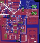
Hey, thanks for the feedback! Sorry if I was confusing in my descriptions. I've attached an image of my board (board) that I working with now. What I was describing was that I was going to run my components and power traces on the top (red). Then on the bottom, I would run my signal layers (solid blue). In the middle would be a ground plane (mesh blue). I have labled my signal ground and power ground polygons. My question was, should I connect the ground planes on the top layer using a trace from vias A to vias B, or should I just let the vias connect to the ground plane for each polygon and that would be their connection together (being tied to the same plane through the vias). Also, you can see the power ground polygon extends a good bit through the circuit so I was wondering if it's better to leave it how it is, or break it up to more localized areas (still connecting to the ground plane through vias).
board.JPG


I've never done a 4 layer board before and like you've said, 2 layer I'd think should be fine. I've done up to 1kW on a 2 layer board with no problems. I do think on those I did a better job of running signals with their respective ground planes beneath.

My problem right now is on the converter shown(board current), it runs fine at 2A. It's a buck converter from 15V to 10V. At 2A output the inductor gets fairly hot, but everything is stable and the output only has about 150mV ripple, peak to peak. As soon as I bump up to 2.5A, the converter duty cycle goes unstable. Now, the output ripple is still the same and the voltage is constant. If I turn off the load and then start it again, it will run fine for a little bit, then the Vds spikes at turn on and turn off begin to decrease and then then duty goes unconstant again. When it shuts down, it keeps the 2.5A at the load, but the voltage is 0.9V.
board_current.JPG

The other converter I'm having trouble with is a boost from 3.6V to 9V at 3A. It does ok at 1A out but it seems jittery (looking at Vds). If I start the supply voltage at 4.2V it pulls it down to 3.4V. If i adjust it back up and step up the load to 2A it might pull it down again, but if it happens to work, the supply voltage will jump back up to 4.2V plus the amount I had to ajust it to get it back there the first time. It seemed adding an RC snubber helped (couple of 603 components running over the mosfet body :roll:). I also added a larger electrolytic capacitor in parallel with the ceramic (on top of the IC) across Vin. I have been able to get it to work from time to time but only if i start at 4.2V and then once it's working, i can drop it to 3.6 and pulse the load just fine. When it drops the input voltage, the output current still meets what I want, but the voltage is no longer 9V but about 3.6V. I will say, the layout on this is pretty poor as well and could be a good bit of my problem.
board_current2.JPG

My power supply is capable of delivering the full load power. I'm using about 1 foot of stranded 14 guage wire twisted together. Only these two converters are populated at the moment and only one works at a time, so there shouldn't be any noise injected from one to the other.
 

Update: I went ahead and replaced the power supply to the last shown circuit with a lithium cell and it works beautifully off of the battery. Not sure what was causing a problem using a power supply though. Still can't get the first converter working for long periods. It may be a heat issue or poor grounding issue. Any thoughts?
 

I think before looking too critically at the layout, you should give some detailed schematics (with component values) so we can see if there are any circuitry-oriented explanations for what you're seeing. I work with eagle so if you want you can just post the files.
 

It will not allow me to upload the file...says it's invalid.

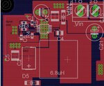
This is a screen shot of the problem converter.
schematic.JPG
 

Thanks for taking the time to give feedback on this! It appears it was a layout issue for the Buck converter (above schematic). I tried stacking inductors and that helped run it a little longer but they were still getting hot and it was still shutting down. I noticed the IC was getting waaay too hot! When I put the end of a flat head screw driver on the package and/or blew on it, I could see the signal quality improving. As I removed it, I could see it start to fail again. I suppose I need a lot more vias near and on the ground pad of the device and maybe a larger surface area inductor.
 

What do you mean by "stacking inductors"?

It sounds like it's just a thermal issue, which isn't really a "layout" issue per say (at least from a circuitry perspective). The MSOP package you're using has an exposed body package; you have soldered that securely to the vias underneath, right? That pad is where most of the dissipated heat from IC is meant to escape. Those vias should carry heat to a ground plane on the opposite side of the board. Inner ground planes won't help much with heat dissipation, so make sure there's a decent ground plane on the bottom layer which has low thermal impedance (lots of vias) to the ground plane directly under the IC.

And it's probably advisable to put an actual rectangular pad for the IC thermal pad, as opposed to the group of vias. It's difficult to get a big pad to form a good solder joint with a bunch of holes. Using a solid rectangular pad surrounded by ground vias should be better. Best of all is using small vias inside the pad.
 

By stacking inductors I mean i put a second one on top of the board mounted one and then soldered their leads together.

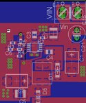
Well that was the trouble i had i think. I had a ground pad on the board as per the data sheets layout guide, but I only had 2 vias next to the IC (As shown in my second board layout image). On top of that the ground pad had thermals enabled so there really wasn't much ground connection I suppose.

On the next board, I have the same ground pad, but I have 6 vias on that ground pad and another 4 above the IC and 6 below (speaking in the Y axis, not Z).

The entire bottom layer of the board is a ground plane. Only a few traces go through that layer.
 
Last edited:

Oh, I was looking at the first image, not the second. Yeah that's definitely no good, you don't want any thermals on that pad.

Keep in mind that Eagle doesn't support via-in-pad when making components (as far as I know, it will always give DRC errors and sometimes screw up the solder mask). The only way I've found to get it to work while keeping eagle happy is to not draw any body pad in the component footprint. Then when you place the footprint in the layout editor, you run a ground plane underneath it, and manually create a stopmask rectangle underneath it with the shape of the body pad. Then you can drop vias inside that "pad" and eagle won't mind. It is a bit of a hassle though.
 

Hmm, I may have a problem then. I just built the part, added it to the schematic, then in the board layout, I added in vias manually and named them the same as the ground polygon. Will this not work?

Thanks for the info!
 

Hmm, I may have a problem then. I just built the part, added it to the schematic, then in the board layout, I added in vias manually and named them the same as the ground polygon. Will this not work?

Thanks for the info!
Doing it that way results in an overlap error on the DRC, at least when I do it. However, it may very well generate gerber files just fine. Make sure you look at the stopmask and copper layers in the gerbers, and also the drill output, to make sure everything is as it should be.
 

I did get DRC errors, but ignored them. The board was made and I have everything on there working now just fine, so I guess that's another way to get vias in the ground pads. The only problem i'm having now is that My converter ICs are getting VERY hot. With a thermocouple leads touching them, I'm getting up to 71deg C after a minute or so. I didn't see just how high it would eventually go. I believe this is a little excessive for an IC even with an integrated MOSFET, am I wrong? They are rated to 125deg C, but can only assure the specs are met up to 85deg C. I put 15mil drills in the ground pads which seems to let some solder through so could it be that the ground connection is not ideal? Is it practical to heat sink an IC?
 

If that's at 15Vin, 10V and 2.5A out at 600KHz, then it's not surprising that it would get that hot. Even if you're only dissipating 5% of the output power in the chip, that's still 1.25W, which will heat up the case by ~40 degrees C above ambient. The junction is probably at around 50 degrees above ambient. Reducing the switching speed is probably the simplest way to improve it.
 

Ah, good point. Thanks! It's that converter and also the battery charger LT3650) that are getting hot. Unfortunately the LT3650 operates at a fixed 1Mhz frequency. It says there is built in protection that reduces the charging current if the temperature approaches 125deg C, so I guess maybe my only option on that one is to reduce the 1.5A charging current a little bit.
 

Status
Not open for further replies.

Similar threads

Part and Inventory Search

Welcome to EDABoard.com

Sponsor

Back
Top