Continue to Site

Welcome to EDAboard.com

Welcome to our site! EDAboard.com is an international Electronics Discussion Forum focused on EDA software, circuits, schematics, books, theory, papers, asic, pld, 8051, DSP, Network, RF, Analog Design, PCB, Service Manuals... and a whole lot more! To participate you need to register. Registration is free. Click here to register now.

GNSS Module Circuit Design

Status
Not open for further replies.
Hello Everyone
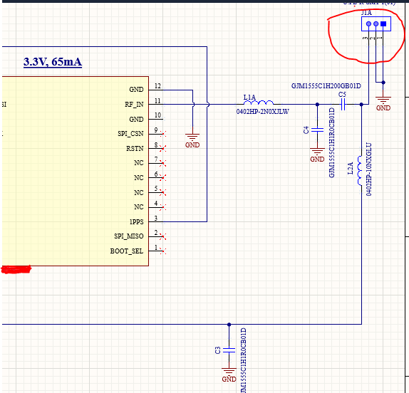
I am trying to design a GNSS receiver circuit to bias 3.3V to the RF feed port (J1A as circled in red) to be used for my active antenna
I am not confident with the biasing circuit design because I picked it from internet. I humbly need your valuable comments to be able to achieve better circuit design for my project. Thanks in advance
1668049664551.png
 

It looks OK electrically provided that L2A exhibits high impedance at the GNSS frequencies. It would be wise to ensure there is something on the feed (the one with C3 across it) to limit the current in case the antenna input is shorted. Layout is critical!

Brian.
 
  • Like
Reactions: Bosssukena

    Bosssukena

    Points: 1
    Thanks for the feedback comment. I was also trying to design something similar and is clear to me now what i have to do to make my circuit better than originally considered😊
Hi,

I saw your picture already.
But you say you found it in the internet, thus I was asking for the internet page.

Klaus
 
Status
Not open for further replies.

Similar threads

Part and Inventory Search

Welcome to EDABoard.com

Sponsor

Back
Top