PhdSA
Newbie level 5

I'm designinig a 3 bit binary differential current steering DAC using differential tansmission gate as a switch.
Below the architecture of the differential switches:

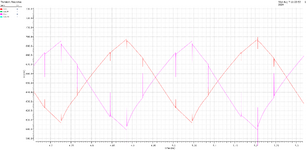
I do the layout in cadence of this subcircuit, however there are a glitch which produce distortion of signal.I need some advices how to connect the binary input (in1n and in1p) in orde to reduce the glitch and avoid distorsion of signal as seen in figure below

Below the architecture of the differential switches:
I do the layout in cadence of this subcircuit, however there are a glitch which produce distortion of signal.I need some advices how to connect the binary input (in1n and in1p) in orde to reduce the glitch and avoid distorsion of signal as seen in figure below