gowthaman90.d
Newbie level 3

Hi all,
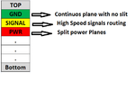
I have a doubt in giving the reference to the signals in High speed PCB. I am working on 16 layer board. My stack up is as below. I have a plan to route the high speed signals in L3. There is continuous GND plane in L2 but I cant give continuous power plane in L4 as the designs have many powers. My high speed signals are crossing over the split power planes in L4. I know the return path of the signals will take the least inductance path.
Will the Split planes in L4 affects the Impedance and Return of the signals in L3?. Experts pls clear me on this.
L1 - TOP
L2 - GND(Continuous plane with no split)
L3 - SIGNAL1 (High Speed Signals Routing)
L4 - PWR (Split power planes)
.
.
L16

