Continue to Site

Welcome to EDAboard.com

Welcome to our site! EDAboard.com is an international Electronics Discussion Forum focused on EDA software, circuits, schematics, books, theory, papers, asic, pld, 8051, DSP, Network, RF, Analog Design, PCB, Service Manuals... and a whole lot more! To participate you need to register. Registration is free. Click here to register now.

[SOLVED] General SMPS/SEPIC related questions

Status
Not open for further replies.

d123

Advanced Member level 5
Joined
Jun 7, 2015
Messages
2,505
Helped
494
Reputation
992
Reaction score
525
Trophy points
1,393
Location
Spain
Activity points
27,148
Hi,

I still have some learning gaps I'm not clearing up.

Regarding inductor selection for SMPS, specifically SEPIC: If a SEPIC CCM design app note formula gives 252uH and the real inductors are +-20% tolerance, does that need to be considered? i.e. A 680uH could range anywhere from 544uH to 816uH, and if the formula says 677uH is needed, is is a good rule of thumb to at least select the next size up, so that at min. tolerance (-20%) and at desired frequency the inductor actually is >677uH? Besides which, should - within reason - let's say another 20% to 40% inductance value be added before selecting one/a pair to avoid saturation?

Regarding N-Channel MOSFET: If Vin to SEPIC is 2.6V to 13.6V, then will the actual VGS (on) on the gate need to be (Vout + Vin) or just Vin to fully turn it on?
Also, it's wishful thinking to hope a guaranteed 1 to 3V on a logic level 40V 11A MOSFET will fully turn on at ~3V when Vin is 13.6V, correct?

Also MOSFET, gate charge level and transition time: IG = QG/t(transition)
Is it best to select nC from the graph including Qgs, Qgd, Qos? as stated in DRIVING THE MOSFET QG and IG Microchip 00786a Does that roughly coincide/correlate with GQtot in the (FDD8447L) NMOS datasheet excerpt.

Transition time: I understand that is user-definable, it's basically waveshaping for speed to cut power losses, so long as the SMPS frequency is not faster than the MOSFET can turn on or off. Is that definition about right for a beginner?

When using rise time and/or fall time in formulas (such as the above about QG/t), do I need to add turn-on delay to rise time, and turn-off delay to fall time?

Is ripple voltage seen on top of Vout? Could 188mV ripple on a 5V out be considered "high" and improvable?
qg and t questions.png

Thanks
 

you are over-complicating your design, in operation the fet is ON or OFF, logic level fets need 5V to be on properly ( some are 3v3 - check the data sheet) the one you show above is 10V for fully on. Put a zener on the gate as overvolts will kill the fet.

The choice of choke is less critical that you might think - as long as it can handle the peak current without magnetic saturation, and the wire losses are low enough you are OK - smaller chokes will give you a wider power bandwidth and allow faster control.

The fet drain sees Vin + Vout in a std sepic, as does the o/p diode, the fet also sees Iin + Iout, as does the o/p diode - so don't skimp on the silicon when designing - a good rule of thumb for newbies is to rate the diode as to the peak current it sees, and the FET rating = 2x the peak current it sees ( or larger for reduced dissipation).
Use a schottky diode (45V) if possible - lower Von and hence losses - also faster to turn off (& on).

You should be spending most of your time mastering the control - sepic is a delayed action converter ( RHP zeroes ), when you suddenly turn the fet on for longer the Vout actually dips initially, before recovering - this action means the control must be generally slower than for other direct action converters ( e.g. buck derived)

You will need "phase lead" or speed up circuits to get the best transient performance, i.e. RC across the input sensing (volts) resistor, and extra damping in the control loop.

The control response should be in the few hundred Hz region - if you have large chokes and output caps.

As to ripple, 188mV rms on 5V is a trifle high, use better electrolytics (lower ESR) and consider a post filter 3.3uH and 220uF (low ESR) - this should take it down

Good luck.

- - - Updated - - -

p.s. your device FDD8447L seems to need at least 4V to be getting close to fully on - it will run at 3v3 / 0 but a little lossily

- - - Updated - - -

p.p.s. at Vin = 2.6V you might get the mosfet to switch (if there are no volt losses in your control / driving circuitry) but it will be a close thing ( and batch dependent ) if it did manage to work you need to take some of the output volts and route this to your control / driver to give it a stable 5V say to run and drive the fet... - without feeding power to your input line ...!!!
 
  • Like
Reactions: d123

    d123

    Points: 2
    Helpful Answer Positive Rating
Is it best to select nC from the graph including Qgs, Qgd, Qos? as stated in DRIVING THE MOSFET QG and IG Microchip 00786a, Does that roughly coincide/correlate with GQtot in the (FDD8447L) NMOS datasheet excerpt.
Yes. Qod=Qg(tot)-(Qgs+Qgd)

Transition time: I understand that is user-definable, it's basically waveshaping for speed to cut switching power losses, so long as the SMPS frequency is not faster than the MOSFET can turn on or off. Is that definition about right for a beginner?
Yes. I have added a word in your sentence above.

When using rise time and/or fall time in formulas (such as the above about QG/t), do I need to add turn-on delay to rise time, and turn-off delay to fall time?
Current is being taken from the driver during the delay time also and is accounted within the first part of Qgs. If you do not want to account for it, subtract that charge from Qg.

Microchip's formula (transition time=Qg/Ig) is valid only if you are driving the gate with constant current (Ig=constant).
 
  • Like
Reactions: d123

    d123

    Points: 2
    Helpful Answer Positive Rating
Hi, thanks a lot.

You should be spending most of your time mastering the control - sepic is a delayed action converter ( RHP zeroes ), when you suddenly turn the fet on for longer the Vout actually dips initially, before recovering - this action means the control must be generally slower than for other direct action converters ( e.g. buck derived)

You will need "phase lead" or speed up circuits to get the best transient performance, i.e. RC across the input sensing (volts) resistor, and extra damping in the control loop.

The control response should be in the few hundred Hz region - if you have large chokes and output caps.

Is a SEPIC type 3 compensation? (I did the calculations for the SEPIC circuit myself but turned to Power Stage Designer to see what it said, and it tells me where RPHZs are) If Power Stage Designer says worst case RHPZ is 850Hz (other at ~7kHz), is - with type 2 compensation - placing a zero at 600Hz okay? And where does pole need to be placed - above the switching frequency or in the above case could 10k or 50kHz suffice?

This is second time around for trying to understand SMPS via a SEPIC and yet again I sometimes wonder if a buck converter isn't perhaps a simpler entry point for a beginner who's just curious but would also like to make the thing and see it work correctly.


p.s. your device FDD8447L seems to need at least 4V to be getting close to fully on - it will run at 3v3 / 0 but a little lossily

p.p.s. at Vin = 2.6V you might get the mosfet to switch (if there are no volt losses in your control / driving circuitry) but it will be a close thing ( and batch dependent ) if it did manage to work you need to take some of the output volts and route this to your control / driver to give it a stable 5V say to run and drive the fet... - without feeding power to your input line ...!!!

I'm going to cheat and return to the original circuit option which had a Vin min of ~4.6V, looking at preliminary calculations and what PSD says, it seems to resolve a few issues, so that's a help. Anyway, thank you very much, your comments are very insightful and have cleared up a few doubts/lagoons of ignorance I still had.

- - - Updated - - -

Hi CataM, thanks very much, and for the excellent word addition.

Current is being taken from the driver during the delay time also and is accounted within the first part of Qgs. If you do not want to account for it, subtract that charge from Qg.

What do you mean by "if you don't want to account for it," wouldn't it be better to include that time/charge in all calculations?

Microchip's formula (transition time=Qg/Ig) is valid only if you are driving the gate with constant current (Ig=constant).

I'm not following you. The gate current is constant, just for a very short amount of time, periodically ;). What exactly do you mean? It was used in this formula for switch power dissipation:

snva168 QPD formula.PNG
 

This is second time around for trying to understand SMPS via a SEPIC and yet again I sometimes wonder if a buck converter isn't perhaps a simpler entry point for a beginner who's just curious but would also like to make the thing and see it work correctly.

Sepic's can be hard to master, are you using a combined choke or separate? if combined it pays to have the windings separated to allow some leakage L - this greatly contributes to proper behaviour of the power stage.

Near light load is the worst case for control - for 850 Hz RHPZ, I would suggest a 200Hz pole in the control - with damping, and a 850Hz phase lead RC in the volt sense line.

Are you using current mode control sensing in the mosfet source? or just plain volt mode? a current mode approach gives a more robust system and can help with control issues. You should have a hardware limit on the max PWM, a bit higher than that which you need at full power and min Vin.
 
  • Like
Reactions: d123

    d123

    Points: 2
    Helpful Answer Positive Rating
What do you mean by "if you don't want to account for it," wouldn't it be better to include that time/charge in all calculations?
You asked: When using "Qg", do I need to add turn on/off delay time ? Yes, you need because you are using Qg.
If you do not want to add the delay time, you will get the same result, but you can not use Qg, instead, you need to use Qfrom threshold to plateau+Qgd+Qod. (notice that the sum of this charges is NOT Qg, but a bit less).
The gate current is constant, just for a very short amount of time, periodically
Microchip and post #1 imply that Ig is constant throughout the whole switching time, which is incorrect. Post #4 attachment, by contrast, implies Ig is constant during the Qgd charge period, which is correct.

Regarding your claim, after you build the SEPIC converter, measure the gate current and see that the gate current decays, then stays constant, then decays again. So if you are picturing the gate current as a constant rectangular pulse, is wrong.
 
  • Like
Reactions: d123

    d123

    Points: 2
    Helpful Answer Positive Rating
Hi,

Separate inductors, and that's an interesting tip about leakage L, thanks.

Thanks for telling me frequencies for compensation.

CMC - VCM but by now, after reading so many times in smps or control/compensation app notes - yourself included in the last post - besides one or two things, CMC seems the more effective solution of the two so I might just redesign the control loop a bit and try to make that work instead.

I don't expect to understand much of the more complex concepts and maths I read about regarding poles and zeroes, or how to insert the square root of -1 into an equation when the calculator I use won't allow that input...but it would be really, really nice to find an app note that explores new territory besides buck/boost/buck-boost design and or compensation and discusses SEPIC VCM compensation for people far below the level of Ray Ridley or Dr. Vorperian. Ironically, the snva168e app note for SEPIC design has CMC compensation, but I think the formulas are for use with a specific driver IC in the design example.

"You should have a hardware limit on the max PWM, a bit higher than that which you need at full power and min Vin." - What is a hardware limit on max. PWM in literal terms, circuit block-wise, please?

Thanks so much for the explanation about Qg and so on. Also, pointing out that that formula is an over-simplification. I was only kidding about the IG pulse shape, but thanks for describing it as I had thought it would be a steep trapezoidal pulse, so thanks again for that description - Do you mean like in the Lazlo gate drive app note timing graph with t1 to t4 for on and off that appears in the first few pages somewhere?
 

Do you mean like in the Lazlo gate drive app note timing graph with t1 to t4 for on and off that appears in the first few pages somewhere?
Yes.

the snva168e app note for SEPIC design has CMC compensation, but I think the formulas are for use with a specific driver IC in the design example.
No. Formulas are for the specified SEPIC converter and the compensation network formulas are widely known as they are Type II compensation with OTA (see here).
 
Last edited:
  • Like
Reactions: d123

    d123

    Points: 2
    Helpful Answer Positive Rating
hardware limit on max PWM, a circuit that limits the maximum PWM drive, irrespective of other elements, for example to 80% ...

- - - Updated - - -

regarding gate drive, depending on your output diode you may want to turn on the fet a bit slower, i.e. 5V drive via 22 ohms, but turn off quickly with a PNP xtor and no gate resistor.
 
  • Like
Reactions: d123

    d123

    Points: 2
    Helpful Answer Positive Rating
Hi,

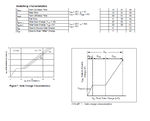
Could someone be able to tell from a few graphs which op amp is most suitable re gbw and V/uS for a 90 kHz smps (sepic), with a crossover frequency of 227Hz? I still don't fully understand what I'm reading and seeing in op amp datasheets, so adult advice would be appreciated. My hunch is the OPA376 is too slow but the OPA322 is fast enough. Image is graphs and characteristics for F and GBW and Vout at xF. Which is suitable, please?

OPA322 and OPA376 gbw slew rates phase gain comparison.png

Compensation: I am having a recurring problem with two of the four equations (2, Z2 and 3, P1) because it feels/sums in the calculator like either a capacitor and/or a resistor has to be small in equation 2 - yet large in equation 3 and I can't seem to square that circle without breaking "cardinal rule" of Ri1 >> Ri2. Also, solutions to Ri1 >> Ri2 (e.g. by making Ri1 30 MegaOhms, Ri2 10 or 100k or whatever minute parallel value) seem to have a negative effect on other equation results. What may I be doing wrong in my approach to resolving the compensation equations correctly and complying with divider resistor and Ri2 rule, please, if you can think of anything?

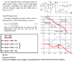
I can get valid zero and pole points with components in calcuations whose results look acceptable in my ignorance, e.g. Z1 = 227Hz, Z2 = 16.6kHz, P1 = 50kHz, P2 = 113kHz for a circuit that has a RHPZ at 0.85kHz (according to Power Stage Designer so I believe it to be true) and then the other at ~7.5kHz at Vin max. Maybe my placing of poles and zeroes is not so good, please feel free to tell me if I'm not putting them in the right places, if that can be understood from brief description provided. Thanks. Below is a summary of the document, the attached PDF, I have taken the type 3 calculations/equations from. It's for buck/boost/buck-boost compensation, but I'm assuming the formulas are equally valid for a sepic as they only relate to the OA compensation, not the switching circuitry. Tried to provide sufficient info, sorry for seeming verbose. Thanks.

type 3 info.png


View attachment Practical-Feedback-Loop-Design-Considerations-for-Switched-Mode-Power-Supplies.pdf
 

Could someone be able to tell from a few graphs which op amp is most suitable re gbw and V/uS for a 90 kHz smps (sepic), with a crossover frequency of 227Hz? I still don't fully understand what I'm reading and seeing in op amp datasheets, so adult advice would be appreciated. My hunch is the OPA376 is too slow but the OPA322 is fast enough.
Crossover freq does not help in selecting OP amp.
Selecting the OP Amp you only care about the "Compensation transfer function" (look into the blue curve in the picture you attached). You need to have an OP Amp with GBW>wcp2*gain between wcp1 and wcp2 (in the image example you attached above is about 25 dB the gain I am talking about). Choose OP Amp with GBW at least 10 times higher than the value you calculated.

What may I be doing wrong in my approach to resolving the compensation equations correctly and complying with divider resistor and Ri2 rule, please, if you can think of anything?
I can't see any problem. Document is not breaking any "rule"...
Z1 and P2 use the capacitors from the "rule" , P2 will be at higher freq than Z1 --> correct.
Z2 and P1 have nothing to do with the capacitors already mentioned. Simply choose resistors from the rule and calculate corresponding capacitors.
 
  • Like
Reactions: d123

    d123

    Points: 2
    Helpful Answer Positive Rating
Status
Not open for further replies.

Part and Inventory Search

Welcome to EDABoard.com

Sponsor

Back
Top