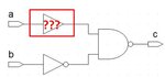
gates delay balancing????
- Thread starter bahare_gh
- Start date
- Status
- Not open for further replies.

mail4idle2
Full Member level 4

What ever you do you cannot match the delay of buffer with inverter. On silicon you cannot guarantee that.

rahdirs
Advanced Member level 1

@bahare_gh: You can make a buffer with a even chain of inverters.
Electrical effort of inverter = Cin(nand)/Cb; Electrical effort of buffer = Cin(nand)/Ca;parasitic delay of inverter = pinv;Logical effort of inverter = 1.
Delay = gh + parasitic delay.
If Ca = Cb, then delay inv. = h + pinv; delay buffer = n.(h)^(1/n) + npinv(min.n=2);
Delay's cannot not equal.you cannot design such a buffer.
But if Ca not equal to Cb,then delay inv. = (Cnand/Cb) + pinv.; delay buffer. = n.(Cnand/Ca)^(1/n) + npinv.
So, setting n(Cnand/Ca)^(1/n) + npinv. = Cnand/Cb + pinv.
So,substituting values ideally you can calculate buffer'size when Ca > Cb.
Last edited:
bahare_gh
Newbie level 4

thank you very much, but can you tell me what are these parameters??
Cin(nand) , Cb , Ca , pinv , gh , h , n , h , npinv , Cnand , pinv , p , C ?????
I guess some of these parameters, but asked it again to ensure.
for mor information: I use the HSpice for project and parameter of transistors are listed below:
_VDD=1.8
C_load out 0 1f
NMOS W=1u L=.18u
PMOS W=3u L=.18u
.MODEL NMOS (LEVEL = 49
+VERSION = 3.1 TNOM = 27 TOX = 4.1E-9
+XJ = 1E-7 NCH = 2.3549E17 VTH0 = 0.3932664
+K1 = 0.5826058 K2 = 6.016593E-3 K3 = 1E-3
+K3B = 1.4046112 W0 = 1E-7 NLX = 1.755425E-7
+DVT0W = 0 DVT1W = 0 DVT2W = 0
+DVT0 = 1.3156832 DVT1 = 0.397759 DVT2 = 0.0615187
+U0 = 280.5758609 UA = -1.208176E-9 UB = 2.159494E-18
+UC = 5.340577E-11 VSAT = 9.601364E4 A0 = 1.7852987
+AGS = 0.4008594 B0 = -3.73715E-9 B1 = -1E-7
+KETA = -1.136459E-3 A1 = 2.580625E-4 A2 = 0.9802522
+RDSW = 105.472458 PRWG = 0.5 PRWB = -0.2
+WR = 1 WINT = 0 LINT = 1.571909E-8
+XL = 0 XW = -1E-8 DWG = -7.918114E-9
+DWB = -3.223301E-9 VOFF = -0.0956759 NFACTOR = 2.4447616
+CIT = 0 CDSC = 2.4E-4 CDSCD = 0
+CDSCB = 0 ETA0 = 2.489084E-3 ETAB = -2.143433E-5
+DSUB = 0.0140178 PCLM = 0.7533987 PDIBLC1 = 0.1966545
+PDIBLC2 = 3.366782E-3 PDIBLCB = -0.1 DROUT = 0.7760158
+PSCBE1 = 8E10 PSCBE2 = 9.204421E-10 PVAG = 5.676338E-3
+DELTA = 0.01 RSH = 6.5 MOBMOD = 1
+PRT = 0 UTE = -1.5 KT1 = -0.11
+KT1L = 0 KT2 = 0.022 UA1 = 4.31E-9
+UB1 = -7.61E-18 UC1 = -5.6E-11 AT = 3.3E4
+WL = 0 WLN = 1 WW = 0
+WWN = 1 WWL = 0 LL = 0
+LLN = 1 LW = 0 LWN = 1
+LWL = 0 CAPMOD = 2 XPART = 0.5
+CGDO = 7.83E-10 CGSO = 7.83E-10 CGBO = 1E-12
+CJ = 9.969364E-4 PB = 0.8 MJ = 0.376826
+CJSW = 2.618614E-10 PBSW = 0.8321894 MJSW = 0.1020453
+CJSWG = 3.3E-10 PBSWG = 0.8321894 MJSWG = 0.1020453
+CF = 0 PVTH0 = -1.428269E-3 PRDSW = -4.3383092
+PK2 = 8.440537E-5 WKETA = 2.341504E-3 LKETA = -9.397952E-3
+PU0 = 15.2496815 PUA = 5.74703E-11 PUB = 1.593698E-23
+PVSAT = 857.5761302 PETA0 = 1.003159E-4 PKETA = -1.378026E-3)
.MODEL PMOS (LEVEL = 49
+VERSION = 3.1 TNOM = 27 TOX = 4.1E-9
+XJ = 1E-7 NCH = 4.1589E17 VTH0 = -0.4045149
+K1 = 0.5513831 K2 = 0.0395421 K3 = 0
+K3B = 5.7116064 W0 = 1.003172E-6 NLX = 1.239563E-7
+DVT0W = 0 DVT1W = 0 DVT2W = 0
+DVT0 = 0.6078076 DVT1 = 0.2442982 DVT2 = 0.1
+U0 = 116.1690772 UA = 1.536496E-9 UB = 1.17056E-21
+UC = -9.96841E-11 VSAT = 1.324749E5 A0 = 1.9705728
+AGS = 0.4302931 B0 = 2.927795E-7 B1 = 6.182094E-7
+KETA = 2.115388E-3 A1 = 0.6455562 A2 = 0.3778114
+RDSW = 168.4877597 PRWG = 0.5 PRWB = -0.4990495
+WR = 1 WINT = 0 LINT = 3.029442E-8
+XL = 0 XW = -1E-8 DWG = -3.144339E-8
+DWB = -1.323608E-8 VOFF = -0.1008469 NFACTOR = 1.9293877
+CIT = 0 CDSC = 2.4E-4 CDSCD = 0
+CDSCB = 0 ETA0 = 0.0719385 ETAB = -0.0594662
+DSUB = 0.7367007 PCLM = 1.0462908 PDIBLC1 = 2.709018E-4
+PDIBLC2 = 0.0326163 PDIBLCB = -1E-3 DROUT = 9.231736E-4
+PSCBE1 = 1.060432E10 PSCBE2 = 3.062774E-9 PVAG = 15.0473867
+DELTA = 0.01 RSH = 7.6 MOBMOD = 1
+PRT = 0 UTE = -1.5 KT1 = -0.11
+KT1L = 0 KT2 = 0.022 UA1 = 4.31E-9
+UB1 = -7.61E-18 UC1 = -5.6E-11 AT = 3.3E4
+WL = 0 WLN = 1 WW = 0
+WWN = 1 WWL = 0 LL = 0
+LLN = 1 LW = 0 LWN = 1
+LWL = 0 CAPMOD = 2 XPART = 0.5
+CGDO = 6.54E-10 CGSO = 6.54E-10 CGBO = 1E-12
+CJ = 1.154124E-3 PB = 0.8414529 MJ = 0.406705
+CJSW = 2.50766E-10 PBSW = 0.8 MJSW = 0.3350647
+CJSWG = 4.22E-10 PBSWG = 0.8 MJSWG = 0.3350647
+CF = 0 PVTH0 = 2.252845E-3 PRDSW = 7.5306858
+PK2 = 1.57704E-3 WKETA = 0.0355518 LKETA = 7.806536E-3
+PU0 = -1.6701992 PUA = -5.63495E-11 PUB = 1E-21
+PVSAT = 49.8423856 PETA0 = 9.968409E-5 PKETA = -3.957099E-3)
rahdirs
Advanced Member level 1
NMOS W=1u L=.18u
PMOS W=3u L=.18u
Are the sizes of all NMOS & PMOS in the whole schematic same??? If so,you can't design such a buffer.(or) did you size the remaining transistors and the above sizes are of the 1st transisitor ??
Cin(nand) - input capacitance of nand gate
Cb - input capacitance of inverter
Ca - input capacitance of buffer
pinv- parasitic capacitance of inverter
g - logical effort
h - electrical effort
n - number of stages(if i implement a buffer with 2 inverters,n = 2;if i do it with 4 inverters,n=4)
Last edited:
rahdirs
Advanced Member level 1
Cb, Ca, pinv???
First for sake of understanding forget about sizes in your simulation.
1) In an inverter if W is NMOS width,then you put PMOS width as 2W/2.5W(mobility of electrons is twice that of holes) to keep drive capability same.
2)We know that capcitance is ∝ width,so in inverter in 1) Cin of inverter is ∝ Wnmos + Wpmos = W + 2W = 3W.
3) In a 2-input NAND gate,the 2 NMOS are in series & PMOS in parallel,so NMOS width is doubled from W to 2W,so as to reduce Ron by half. Hence, Cin(nand) ∝ Wnmos +Wpmos = 2W +2W = 4W.
4)The parasitic delay(p)expresses the intrinsic delay of the gate due to its own internal capacitance, which is largely independent of the size of the transistors in the logic gate.The principal contribution to the parasitic capacitance is the capacitance of the diffused regions of transistors connected to the output signal. The capacitance of these regions will depend on their layout geometry and on process parameters.
Generally pinv. is taken as 1
5) Now in your case Cb is input capacitance of inverter of Pmos width 3.0u & Nmos width 1u. Hence,Cb ∝ 3 + 1 = 4u. U need to know capacitance for some width to remove proportionality const.I'm exactly sure of the value but i think 4.256fF ∝ 2.1u. Thus, Cb = (4/2.1)*4.256fF.
Now,calculate Ca as per second part of post #4, & Cin(nand) as from 3)
Attachments
Last edited:
rahdirs
Advanced Member level 1
@bahare_gh: I got those values during my VLSI Lab Course.
You are not trying to minimize the delay of the entire circuit,are you ?? As you are just trying to keep it glitch free,keep size of nand gates simply higher than that of inverter.
Say, keep width of NMOS in nand gate = 2u & width of pmos = 3u. then you hv cin(nand) ∝ 5u.
Calculate Ca of buffer from post #4 as you now have both C(nand) & Cb,by keeping n even. An even chain of inverter's constitutes a buffer.See if you can get a value for Ca. If no such Ca exists, you cannot create such buffer.
If Ca exists,you can get width of 1st nmos in buffer by ∝ Ca/3 & pmos by ∝ 2Ca/3.
To balance delay, delay of buffer = n(Cnand/Ca)^(1/n) +n*pinv = n(Cnand/Ca)^(1/n) + n;
delay of inverter = (Cnand/Cb) + pinv = (5/4) + 1 = 2.25 units.
Only possible to balance for buffer of minimum size, n is 2 so 2*sqrt(Cnand/Ca) + 2 = 2.25
=> Cnand/Ca = 1/16.
=> Ca = 16 *Cnand.∝ 80u.
Thus size of nmos of first inverter = 80/3 u ,pmos size = 160/3 u.
size of nmos of second inverter = 20/3 u,pmos size = 40/3 u.
From sizes & value of electrical effort(Cnand/Ca) shows how difficult it is to equate delays of buffer & inverter.
- - - Updated - - -
You could've simplified your calculations as both C at the beginning were proportional to 4.256.
Nevertheless, Ca = 120.45fF & u get n = 59.44 = 60(approx.)
Now, as your buffer contains two inverters,
1st inverter: Nmos size = 20u , Pmos size = 40u
2nd inverter:Nmos size = 5.76u,Pmos size = 11.52u
Last edited:
bahare_gh
Newbie level 4
thank you very very much for your replies
- - - Updated - - -
and
It was a simple circuit, do We use the same method for complex circuits ؟؟
I calculate the delay of gates: t(inv)=4.5652E-11 and t(buffer)= 4.7694E-11. these are aqual Approximately. but is it hard to exactly balance them??? the delay defference of 0.2 is not too large??Now, as your buffer contains two inverters,
1st inverter: Nmos size = 20u , Pmos size = 40u
2nd inverter:Nmos size = 5.76u,Pmos size = 11.52u
- - - Updated - - -
how did you get these values??2nd inverter:Nmos size = 5.76u,Pmos size = 11.52u
and
It was a simple circuit, do We use the same method for complex circuits ؟؟
rahdirs
Advanced Member level 1
@bahare_gh: See it is exactly hard to match delay of both.Because inverter had one gate & buffer had 2 inverters in series.You are trying to match the delay of 2 gates in buffer to 1 gate in inverter.
Regarding those values, there is term called Path Effort(F) & stage effort(f) which is used.
For buffer, Path Effort = C(nand)/Ca.
We designed buffer with 2 inverters in series. The input capacitance of 1st inverter = Ca, let's say input capacitance of 2nd inverter = C2 , input cap. of nand gate = Cnand.
stage effort of 1st inv. = C2/Ca,2nd inv. = Cnand/C2
We had Cnand ∝ 5u , Ca ∝ 59.44u ('n' calculated by you) = 60u (approx.)
F = 5u/60u = 1/12.
To minimize delay stage effort of each stage should be equal & their product should be Path effort.
=> f*f = F => f = sqrt(F) = sqrt(1/12) = 0.288.
=> C2 = 0.288*Ca ∝ 17.32 u .
Now,we have Ca ∝ 60u , C2 ∝ 17.32u.
Size of 1st inverter in buffer is calculated from Ca, Wnmos = 60u/3 = 20u , Wpmos = 40u.
SIze of 2nd inv. in buffer is calc. frm C2, Wnmos = 17.32u/3 = 5.773u , Wpmos = 11.547u.
These calculations are known as "Method of logical effort".
Try reading book "Logical Effort
You just need to read 1st chap(hardly 10 pages) to understand this stuff.
After reading 1st chap try implementing inverter with 3 inverters in series & buffer with 2 inverters & use method of logical effort to see how close you can match them
- Status
- Not open for further replies.
Similar threads
-
How to calculate the gate delay in ccs model?
- Started by MonsterLyon
- Replies: 2
-
How modify delay of a lot paths to meet constraints quickly
- Started by nguyenvanthien
- Replies: 8
-
Timing question with combinational gates
- Started by Qwerty112233
- Replies: 4
-
Command in Design Compiler to get least delay
- Started by hw2000
- Replies: 3
-
What is delay cell? Is it just big buffer?
- Started by Collang2
- Replies: 1