azadfalah
Full Member level 2

Hi friends I hope you are great
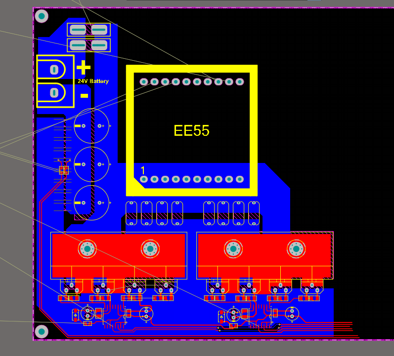
I am designing a full bridge dc / dc converter, please comment on my PCB Layout and Gate Driver
Topology : Full Bridge
Frequency = 50khz
Input : 24V
MAX Input Current: 50A
Output = 350V DC
Power = 1KW
Gate Driver : IR2113
In the previous design, i had a problem with the Vgs Rings
After researching and fixing the bugs, this design is finalized, Please guide me to make it better
*The primary transformer wires are connected directly to the heatsinks

Thanks
I am designing a full bridge dc / dc converter, please comment on my PCB Layout and Gate Driver
Topology : Full Bridge
Frequency = 50khz
Input : 24V
MAX Input Current: 50A
Output = 350V DC
Power = 1KW
Gate Driver : IR2113
In the previous design, i had a problem with the Vgs Rings
After researching and fixing the bugs, this design is finalized, Please guide me to make it better
*The primary transformer wires are connected directly to the heatsinks
Thanks

