Fesch
Newbie

- Joined
- Jun 18, 2020
- Messages
- 3
- Helped
- 0
- Reputation
- 0
- Reaction score
- 0
- Trophy points
- 1
- Activity points
- 53
Hey there,
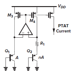
I am currently trying to understand the bandgap reference circuit shown in the figure below. I am specifically trying to understand how to determine the needed open-loop voltage gain of the op amp.
The MOSFETs are supposed to be biased in saturation region and strong inversion. Ideally, the op amp input voltage difference should be zero. But in reality there will always be an offset voltage, even though the op amp inputs might be chopped to reduce the offset, the mismatch between the PMOS in the current mirror is still existent.
Assume that the maximum offset voltage (or error) at the input of the op amp is \[ V_{os} \]. Which is equal to \( V_{os} = V_{in+} - V_{in-} \). So I can say \( A_v \cdot V_{os} = V_{DD} - V_{SG} \). To make sure that the gain is sufficiently high it has to be larger than the output voltage divided by the input voltage:
\[ A_v > \frac{V_{DD} - V_{SG}}{V_{os}} \]
Is this approach correct? Am I not mixing small-signal analysis values with large-signal analysis values? Or are all those values large-signal values because they define my bias point of the circuit?
Thus, as an example:
\[ V_{DD} = 2 V\\ V_{os} = 500 \mu V\\ V_{SG} = 600 mV\\ A_v > \frac{2V - 0.6 V}{500 \mu V} = 2800 \]
Thanks for your help!

Bandgap reference circuit, figure taken from B. Ravazi - Design of Analog CMOS Integrated Circuits
I am currently trying to understand the bandgap reference circuit shown in the figure below. I am specifically trying to understand how to determine the needed open-loop voltage gain of the op amp.
The MOSFETs are supposed to be biased in saturation region and strong inversion. Ideally, the op amp input voltage difference should be zero. But in reality there will always be an offset voltage, even though the op amp inputs might be chopped to reduce the offset, the mismatch between the PMOS in the current mirror is still existent.
Assume that the maximum offset voltage (or error) at the input of the op amp is \[ V_{os} \]. Which is equal to \( V_{os} = V_{in+} - V_{in-} \). So I can say \( A_v \cdot V_{os} = V_{DD} - V_{SG} \). To make sure that the gain is sufficiently high it has to be larger than the output voltage divided by the input voltage:
\[ A_v > \frac{V_{DD} - V_{SG}}{V_{os}} \]
Is this approach correct? Am I not mixing small-signal analysis values with large-signal analysis values? Or are all those values large-signal values because they define my bias point of the circuit?
Thus, as an example:
\[ V_{DD} = 2 V\\ V_{os} = 500 \mu V\\ V_{SG} = 600 mV\\ A_v > \frac{2V - 0.6 V}{500 \mu V} = 2800 \]
Thanks for your help!
Bandgap reference circuit, figure taken from B. Ravazi - Design of Analog CMOS Integrated Circuits

