Junus2012
Advanced Member level 5

Dear friends,
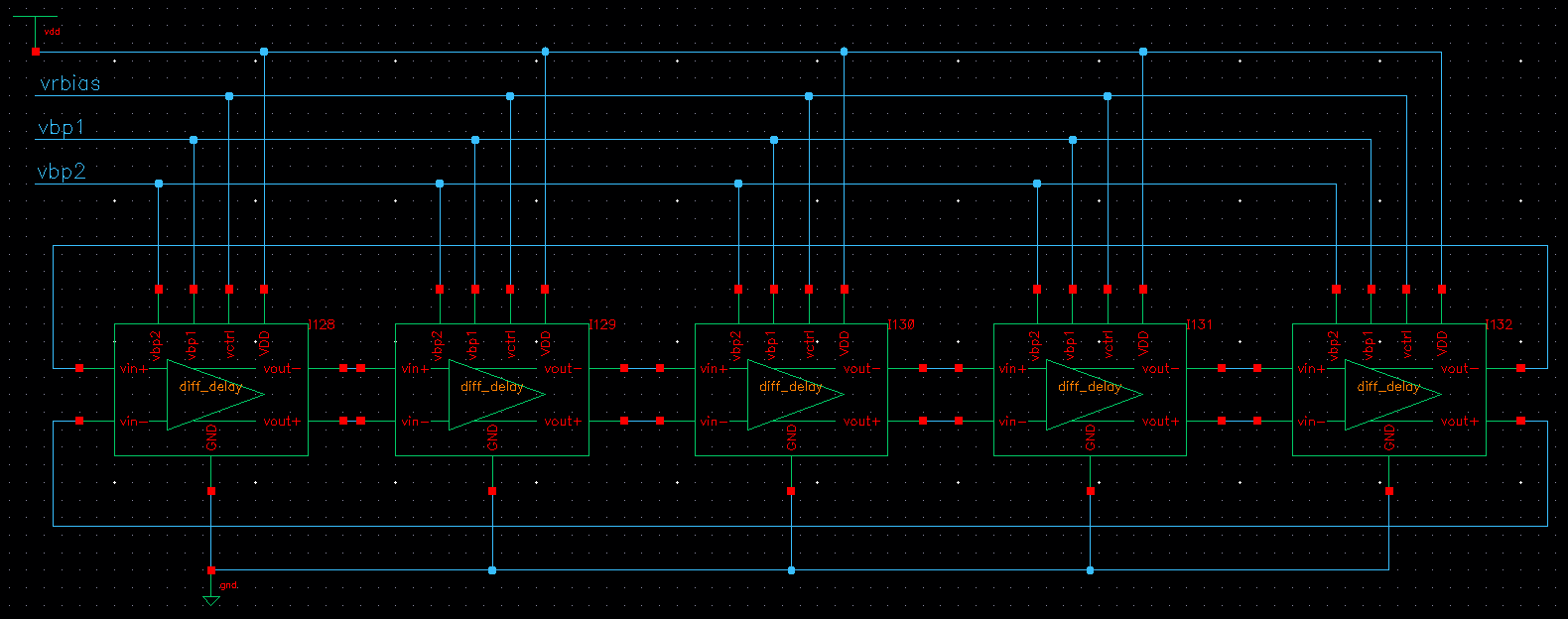
I have designed an odd number fully differential VCO as shown below

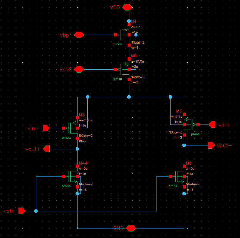
the differential cell is given below (with the transistor sizes)

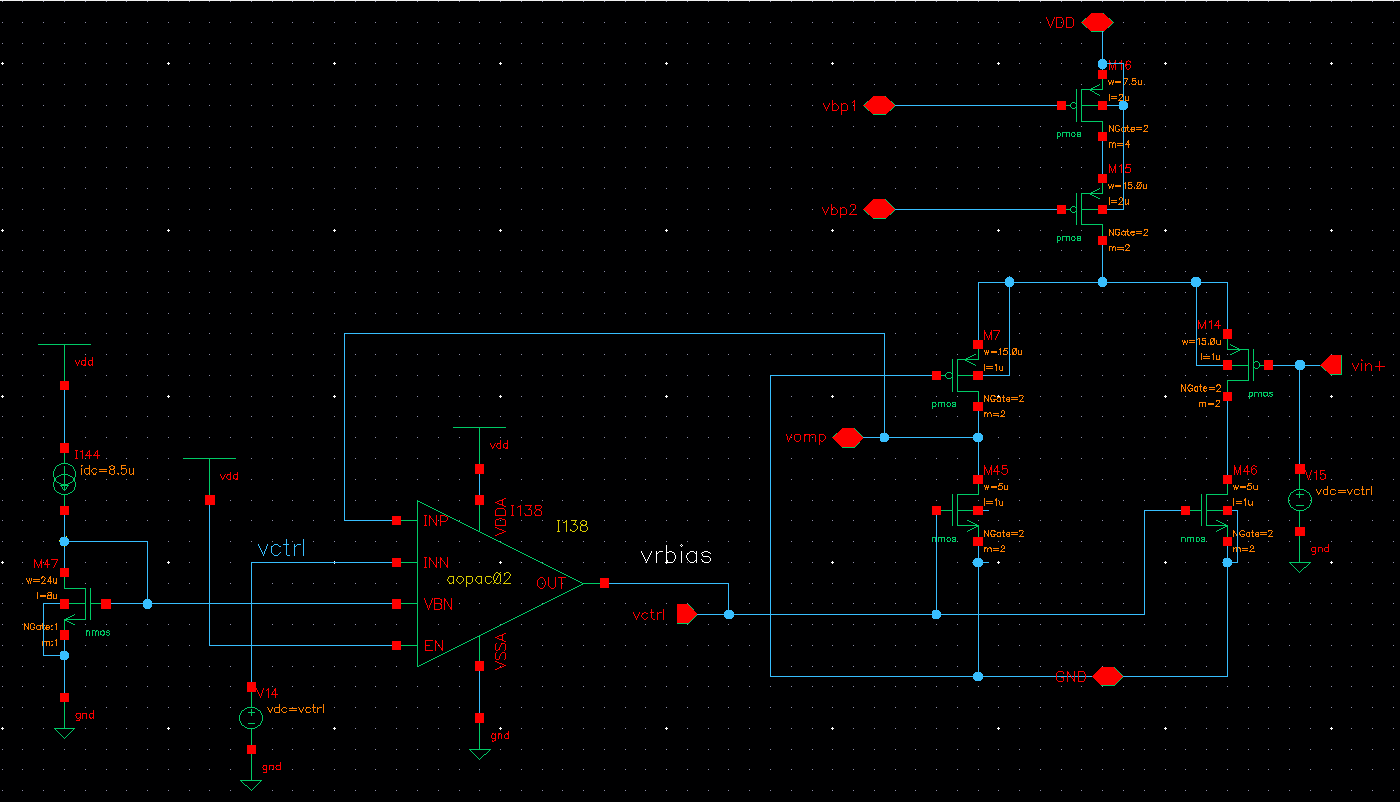
I used replica biasing circuit with feedback loop to bias the delay cells as given below

The loop gain of the op-amp is very large so that I have guaranteed that output voltage is equal to the vctrl (some people call it vref), as exactly explained in literature. However, literature staes that the biased NMOS load of the delay cell are in the triode region, but in my case it is in saturation region. I have tried to change the vctrl to many values but still the load is showing me in saturation.
to confirm the loop functionality, I have sweeped the biasing current in wide range and also by varying the supply voltage, the loop was strong enough to keep to keep the output swing equal to vctrl..
I did another DC simulation to test the steady state circuit of the circuit by applying DC input to the cell and breaking the VCO feedback, looks every cell is working fine like a perfect inverter.
my trouble come with transient simulation, the circuit is not at all oscillating. At the start I thought it is about the intial condition of the simulator but I then used to set the initial condition from the simulation convergence aid, again not working.
the last step in my investigation I replaced the NMOS load transistors with an equivalent equal normal resistors (exctracted from vctrl/actual current), the circuit start to oscillate but with not equal outputs,
I do appreciate your help to solve my problem with the NMOS load,
do you think I have transistors size issue?
Thank you in advance
Regards
I have designed an odd number fully differential VCO as shown below
the differential cell is given below (with the transistor sizes)
I used replica biasing circuit with feedback loop to bias the delay cells as given below
The loop gain of the op-amp is very large so that I have guaranteed that output voltage is equal to the vctrl (some people call it vref), as exactly explained in literature. However, literature staes that the biased NMOS load of the delay cell are in the triode region, but in my case it is in saturation region. I have tried to change the vctrl to many values but still the load is showing me in saturation.
to confirm the loop functionality, I have sweeped the biasing current in wide range and also by varying the supply voltage, the loop was strong enough to keep to keep the output swing equal to vctrl..
I did another DC simulation to test the steady state circuit of the circuit by applying DC input to the cell and breaking the VCO feedback, looks every cell is working fine like a perfect inverter.
my trouble come with transient simulation, the circuit is not at all oscillating. At the start I thought it is about the intial condition of the simulator but I then used to set the initial condition from the simulation convergence aid, again not working.
the last step in my investigation I replaced the NMOS load transistors with an equivalent equal normal resistors (exctracted from vctrl/actual current), the circuit start to oscillate but with not equal outputs,
I do appreciate your help to solve my problem with the NMOS load,
do you think I have transistors size issue?
Thank you in advance
Regards

